324 한국진공학회 TF-P004
Investigating InSnZnO as an Active Layer for Non-volatile Memory
Devices and Increasing Memory Window by Utilizing Silicon-rich
SiOx for Charge Storage Layer
Heejun Park1, Cam Phu Thi Nguyen1, Jayapal Raja1, Kyungsoo Jang1, Junhee Jung2, Junsin Yi*1
1College of Information and Communication Engineering, Sungkyunkwan University, Suwon, 440-746, Korea 2Department of Energy Science, Sungkyunkwan University, Suwon, 440-746, Korea
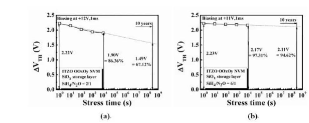
In this study, we have investigated indium tin zinc oxide (ITZO) as an active channel for non-volatile memory (NVM) devices. The electrical and memory characteristics of NVM devices using multi-stack gate insulator SiO2/SiOx/SiOxNy (OOxOy) with Si-rich SiOx for charge storage layer were also reported. The transmittance of ITZO films reached over 85%. Besides, ITZO-based NVM devices showed good electrical properties such as high field effect mobility of 25.8 cm2/ V.s, low threshold voltage of 0.75 V, low subthreshold slope of 0.23 V/dec and high on-off current ratio of 1.25 × 10⁷. The transmission Fourier Transform Infrared spectroscopy of SiOx charge storage layer with the richest silicon content showed an assignment at peaks around 2000-2300 cm-1. It indicates that many silicon phases and defect sources exist in the matrix of the SiOx films. In addition, the characteristics of NVM device showed a retention exceeding 97% of threshold voltage shift after 104 s and greater than 94% after 10 years with low operating voltage of +11 V at only 1 ms programming duration time. Therefore, the NVM fabricated by high transparent ITZO active layer and OOxOy memory stack has been applied for the flexible memory system.
Keywords: memory, NVM, ITZO
ΔVTH (V) Retention Time T2 T3 1s 2.22 2.23 10s 2.15 2.21 100s 2.02 2.20 1000s 1.94 2.18 10000s 1.90 (85.58%) 2.17 (97.31%) 10 years 1.49 (67.12%) 2.11 (94.62%)
Table 1. Memory window of NVM devices after durating of retention (10000 s) and
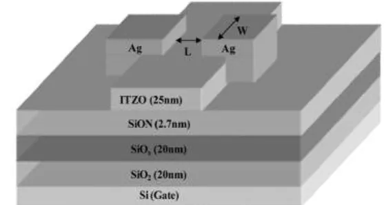
Figure 1. Schematic cross section of the ITZO NVM bot-tom-gate structure with SiO2/SiOx/SiOxNy memory stack on silicon substrates.
제 50 회 동계학술대회 325
Figure 2. (a) Transmission FTIR and optical bandgap of Si-rich SiOx charge storage layer. (b)
Capacitance-voltage measured at retrace mode of OOxOy MIS structure.
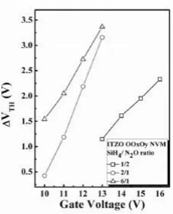
Figure 3. Threshold voltage shift of OOO NVM devices at different operating voltage.
Figure 4. (a) Transfer hysteresis characteristics of OOxOy/ITZO NVM device at different oper-ating voltages. (b) Programming characteristics of NVM device for various programming pulse widths at difference operating voltages.
326 한국진공학회
Figure 5. Retention properties extrapolation up to 10 years of OOxOy/ITZO NVM devices with the gas ratio SiH4/N2O of (a) 2/1 and (b) 6/1 for charge storage layer.