Industry Applicable Future Texturing Process for Diamond wire sawed Multi-crystalline Silicon Solar Cells: A review
11
0
0
전체 글
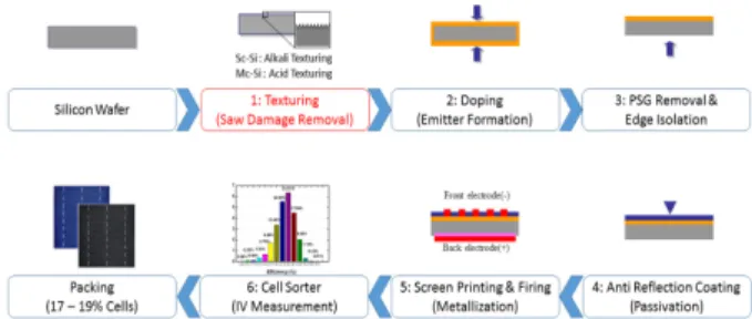
(2) 2. M. Ju et al. / Current Photovoltaic Research 6(1) 1-11 (2018). Fig. 3. Conventional process flow of crystalline silicon solar cells. Fig. 1. The change in solar cell market share from 1980 to 20143).. of the acid chemical are HF and HNO3. The reaction formula for acid texturing is as follow10,11,12). 3Si + 4HNO3 + 18HF → 3H2SiF6 + 4NO + 8H2O. (1). To have an in-depth understanding of the etching mechanism, the chemical reactions has been explained in detail in the below: - HNO3 oxidation The first chemical that acts with silicon is HNO3. HNO3 acts to oxidize the silicon in the reaction with the silicon. Fig. 2. Crystalline silicon wafer fabrication process and production efficiency for each process2).. Si + 4HNO3 → SiO2 + 4NO2 + 2H2O. (2). The by-products of reaction, NO2 and H2O then proceed texturing technologies that could minimize the optical loss of. following chemical reaction.. mc-silicon solar cells are explained. Finally, next generation texturing technology to survive in the fierce cost competition of. 2NO2 + H2O → HNO2 + HNO3. (3). photovoltaic market is discussed. HNO2 produced by the first oxidation proceeds the second. 2. Conventional Texturing Technology for Multi-crystalline Silicon Cells Fig. 3 shows the conventional process flow of crystalline silicon solar cells. For texturing, anisotropic etching is carried out using KOH or NaOH based alkali chemicals. For multi-. oxidation. Si + 4HNO2 → SiO2 + 4NO + 2H2O. (4). The by-products of second oxidation, NO and H2O react with HNO3 which is the final by-product of (2) and (3). 2NO + H2O + HNO3 → 3HNO2. (5). crystalline solar cell fabrication, isotropic etching is carried out using HF and HNO3 based acid chemicals at the first step of. The HNO2 proceeds second oxidation as in eq. (4) thereby. texturing process. Depending on the texturing method, the. repeating the oxidation reaction. The oxidation chain reaction. conventional solar cell process is divided into single and multi-. by HNO2 can be simply expressed as follow.. crystalline. 3Si + 4HNO3 → 3SiO2 + 4NO + 2H2O. (6). 2.1 Mechanism 2.1.1 Chemical Reaction. Generally, isotropic etching using acid chemical is carried out for multi-crystalline wafer texturing. The main ingredients. - HF etching SiO2 formed by oxidation of Si and HNO3 reacts with HF chemical..
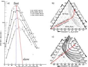
(3) M. Ju et al. / Current Photovoltaic Research 6(1) 1-11 (2018). SiO2 + 4HF → SiF4 + 2H2O. (7). 3. the ratio and diluted solution as seen in Fig. 414,15). As seen in Fig. 4-a), the fastest etching rate occurs when the. The by-product, SiF4 reacts with HF. SiF4 + 2HF → H2SiF6. ratio of HF:HNO3 = 7:3. At this composition, the silicon etching (8). rate decreases when the concentration of HF or HNO3 increases. The solution that contains relatively more HF makes the reaction more fast with reduction in the etching rate and hence. Etching formula of SiO2 by HF is expressed as follows.. this solution is called as HF-rich solution. The solution that SiO2 + 6HF → H2SiF6 + 2H2O. (9). contains relatively more HNO3 causing reduced rate is called HNO3-rich solution.. - HNO3 + HF etching. Silicon wafers are etched to 1 µm using 3 different solution. It can be seen that summing up the etching formulas of. compositions (A:HF-rich, B:Balance, C:HNO3-rich). Fig. 5. crystalline silicon wafer by HNO3 and HF chemical mechanism,. shows the physical characteristic change of the etched silicon. (6) and (9) becomes the etching reaction formula of (1).. surface.. However, away from the theoretical chemical mechanism,. When the silicon is etched with HF-rich solution (A),. reaction like (11) may occur depending on the chemical. vulnerable parts such as saw damage, grain boundary and. composition and environmental impacts such as temperature in. defects are oxidized first. Since HF is always etching the. 13). actual etching . 3Si + 4HNO3 + 18HF → 3H2SiF6 + 4NO + 8H2O. oxidized silicon, the fragile silicon parts are etched in depth (10). 3Si + 2HNO3 + 18HF → 3H2SiF6 + 2NO + 4H2O + 3H2 (11). direction due to the sequential oxidization by nitric acid. In the case of using HNO3-rich solution (C), although vulnerable parts are oxidized first, other normal silicon parts are also oxidized due to the high concentration of HNO3. Since HF etches. For the etching of crystalline silicon wafer using HF and. oxidized surface, the entire surface of the silicon is uniformly. HNO3 solution, oxidation by HNO3 first occurs and then etching. etched in width direction. Solution B has both characteristics of. by HF is carried out. Depending on the chemical ratio of HNO3. solution A and C.. and HF, different etching mechanism occurs physically.. The results of etching characteristics can be confirmed by reflectivity values. As mentioned before, the chemical reaction. 2.1.2 Physical Reaction. of HF and HNO3 etching solution supports the physical reaction. The etch rate of HF and HNO3 etching solution depends on. phenomena and the texture mechanisms can be understood. The. Fig. 4. a) Change in silicon etching rate depending on the composition of HF:HNO314). b) Triangular diagram for the etching rate of silicon as a function of etchant composition in the HF:HNO3:H2O system14). c) Triangular diagram for the etching rate of silicon as a function of etchant composition in the HF:HNO3:CH3COOH system15).. Fig. 5. Physical characteristics of multi-crystalline wafers by etch depth when etched by HF : HNO3 : CH3COOH = A(82:3: 15, HF-rich), B(30:15:55, balanced) and C(10:75:15, HNO3-rich) solutions, SEM 2k..
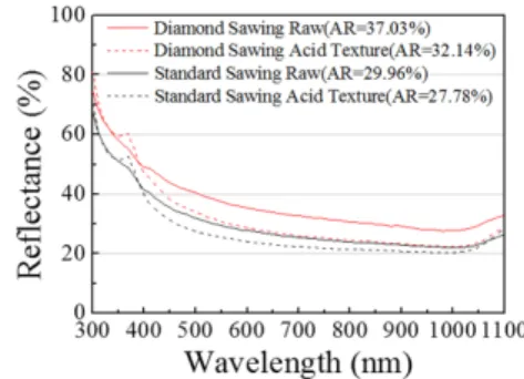
(4) 4. M. Ju et al. / Current Photovoltaic Research 6(1) 1-11 (2018). Fig. 6. Reflectivity values of crystalline wafers by etch depth when etched by HF:HNO3:CH3COOH = A(82:3:15, HF-rich), B (30:15:55, balanced) and C(10:75:15, HNO3-rich) solutions.. popular texturing technique of mc-silicon solar cells first induces oxidation of vulnerable parts such as saw damage, grain boundary and defects by HNO3. A reasonable amount of HF is. Fig. 7. (a) Saw damage and defects on the wafers from a diamond saw, (b) Acid texturing surface from a diamond saw, (c) Saw damage and defects on the wafers from a standard saw, (d) Acid texturing surface from a standard saw.. used to match depth and width etching characteristics to obtain optimal reflectivity values. 2.2 Diamond Saw Wafer Texturing For the crystalline silicon solar cell cost competition, the supply of lower-cost wafers is a matter of life or death for solar cell manufacturing companies. In such a situation, the supply of diamond sawing wafer which is more than 14% cheaper is welcome6). However, a serious problem arises when the diamond sawing wafer is used for conventional mc-silicon solar cell manufacturing process8,16). As seen in Fig. 7(a) and (c), there are less saw damage and defects on the wafers produced by diamond saw compared to the wafers produced by a standard saw. This is a good characteristic that boosts the strength of the wafer and makes it possible to produce thinner wafers. When observing the surface with the naked eye, the wafer produced by standard saw is light grey while the wafer produced by diamond saw is a shiny silver color. The diamond sawing wafer surface makes it difficult to have texturing surface with adequate reduced reflectivity by the acid texturing process used in conventional multi-crystalline solar cells as seen in Fig. 7(b) and (d). Fig. 8 shows that raw surface of diamond sawing mc-Si wafer has about 8% higher average reflectivity in the wavelength rage of 300∼1100 nm compared to that of standard sawing mc-Si wafer. After the acid texturing, diamond sawing mc-Si wafer has about 5% higher average reflectivity compared to that of. Fig. 8. The reflectance variation with respect to diamond and saw wire cut wafers.. efficiency of solar cell’s using diamond sawing wafer is 0.3~ 0.4% lower than that using standard sawing wafer8). The reduction of conversion efficiency is related to the profit and images of solar cell manufacturers and the diamond sawing wafer has not been popular despite the provision of cheap wafers. Solar cell manufacturers need to consider next generation multi-silicon texturing technology for low reflectivity and a production line should be built to use diamond saw wafers. The production of low cost, high efficiency multi-silicon solar cells using next generation multi-silicon texturing technology can put up with the situation where market price is falling further and price competition between solar cell companies is stiff.. 3. Next Generation Texturing Technology for Multi-silicon Solar Cells. standard sawing mc-Si wafer. The high reflectivity acts as a factor to inhibit the conversion. The reflection loss of multi-silicon solar cells is large compared. efficiency of the solar cells. It has been reported that the conversion. to the single silicon solar cells with random pyramid structures1)..
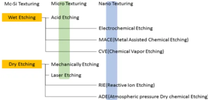
(5) M. Ju et al. / Current Photovoltaic Research 6(1) 1-11 (2018). 5. To reduce the reflection loss, various texturing processes are. carried out. Mechanical etching using dicing saw is then used to. being studied.. get wanted surface shapes. Finally, surface defects formed by. The mc-silicon solar cell texture is divided into micro texture. mechanical etching are removed as seen in Fig. 10. The mc-silicon. and nano texture depending on the texturing size. Depending on. solar produced using the above processes has current improvement. the process method, it is divided into wet etching and dry etching.. of 2.4 mA/cm2 compared to the reference. However, as seen in Fig. 11(a) below, the depth of the V-groove is 65 µm and the. 3.1 Micro Texturing Technology Micro texturing technology reduces the reflectivity of mc-silicon wafer by etching micro scale shapes. Micro technology includes. width is 120 µm and it is too large for screen printing process. Roller printing process techniques as seen in Fig. 11(b), should be introduced to fabricate solar cells19).. honey comb structures and inverted pyramid structures. These. The application of mechanical texturing to mc-silicon solar. structures are implemented by selective etching using etching. cell requires extra process steps and the breakage rate during. 17,18). . However, the process of mask formation, etching. solar cell manufacturing process is high due to low wafer. and removal is complicated and expensive. It is not suitable for. thickness caused because of etching. Thus, it is difficult to. cheap conventional process. Thus to circumvent the problem,. produce conventional mc-silicon solar cells.. masks. selectively etching silicon wafer process such as mechanical etching and laser etching have been attempted.. 3.1.2 Laser Etching. Laser etching technique etches silicon wafer surface using 3.1.1 Mechanically Etching. physical energy like the mechanically etching technique.. Mechanical etching tool, as seen in Fig. 10, consists of a. However, mechanically etching technique etches through direct. cylindrical wheel with a V-grooved surface, over which the. contact while the laser etching technique uses a high energy. abrasive layer made of diamond is coated.. laser light source. The wafer is etched by irradiation to melt the. The research for application to mc-silicon solar cells was. surface of the wafer in a non-contact manner. Since there is no. conducted by Interuniversity Microelectronics Center (IMEC). abrasion of saw, laser etching of the silicon wafers results in. research group in Belgium in collaboration with Konstanz. same quality. Laser light source that can be absorbed by silicon. 19). University in Germany . For application to mc-silicon solar. wafer, should be used for laser etching. A typical laser light. cell, saw damage etching of solar grade silicon wafers are. source is Nd:YAG 1064 nm and through harmonic frequency generation of doubling and tripling, multi laser source of 532 nm and 355 nm can be obtained. Fig. 12 shows the absorption coefficients of crystalline silicon. For the case of 1064 nm IR laser, the energy is distributed. Fig. 9. Technology classification with respect to micro and nano textured surface.. Fig. 10. Schematic of Mechanical Etching tool used for texturing process.. Fig. 11. Roller printing technique used for texturing process.. Fig. 12. The absorption coefficient of crystalline silicon..
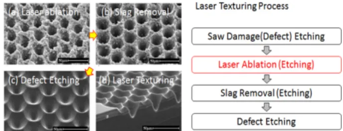
(6) 6. M. Ju et al. / Current Photovoltaic Research 6(1) 1-11 (2018). from a surface to a very deep level by the light absorption. 3.2.1 Reactive Ion Etching (RIE). property of crystalline silicon wafer unlike the V or Green laser.. RIE (Reactive Ion Etching) texturing was developed in 1997. If physical etching is carried out using IR laser, defects may be. and is used for mass production by some mc-silicon solar. formed to deep levels. To solve the problem, the laser is. cells28). Plasma generated during the reactive ion, physichemically. irradiated in the form of an ultrafast pulse of nano, pico and. etches the silicon. In a vacuum chamber, cathode is formed on. femto second minimizing the well level laser damage and the. silicon wafer substrate by RF power and plasma is generated to. system is configured so that energy at the surface is most active.. etch the wafer. When the cation of the particles impacts on the. Fig. 13 shows the texturing process using laser etching.. surfaces of the silicon wafer cathode physically, reaction gases. Saw damage etching is carried out for solar graded wafers. and ions react with silicon, chemically resulting nano texture. and laser ablation is carried to get required surface shapes. Slag. structures. The typical reaction gases are SF6, O2 and Cl2. By. formed on the surface is removed by low concentration of alkali. controlling the gas concentration and ratio, the nano scale. solution such as NaOH. Finally, laser defects remaining on the. surface structures and shapes can be optimized29).. surface is removed through isotropic etching20,21,22).. RIE texturing process begins with acid etching raw silicon. The laser etching technique is widely used for realizing high. wafer to remove saw damages as seen in Fig. 15. The nano scale. efficiency solar cell structures. It is also used for MWT (Metal. surface structures are formed. Finally, a process of removing. Wrap Through)23), EWT (Emitter Wrap Through)24,25) and. damages caused by ion impact of RIE and contaminants is. 26). PERC (Passivated Emitter Rear Contact) . MWT and PERC high efficiency solar cells have been tried for mass production. 2. However, it takes 20 min. to get an area of 8 cm of structures 20). shown in Fig. 13 by texturing using laser etching only . The. carried out30). Recently it has been reported that a mc-silicon solar cell showed efficiency of 18.72% which was 0.6% higher than 18.1%, the efficiency of the reference cell31). RIE texturing. slow process time makes it difficult to apply to mass production vying for seconds. The laser texturing technique is only in research stage due to process time, etc.. 3.2 Nano Texturing Technology Nano texturing surface with nano scale structures shows black color and can also be called black silicon27). As shown in Fig. 14, nano texturing surface has very low reflectivity compared to micro texturing surface. Noticeable improvement of reflectivity is seen in blue response area. Nano texturing technique with very low reflectivity can. Fig. 14. Reflectance variation with respect to micro and nano texturing carried with different process.. define required shapes with very shallow etching and it is suitable for high efficiency next generation conventional texturing technology. Nano texturing etching methods include RIE (Reactive Ion Etching), ADE(Atmospheric pressure Dry chemical Etching), Electrochemical Etching, MACE (Metal Assisted Chemical Etching) and CVE (Chemical Vapor Etching).. Fig. 13. Laser texturing process.. Fig. 15. The variation in etching depth and reflectance of RIE texturing with respect to different gas mixture..
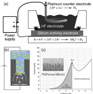
(7) M. Ju et al. / Current Photovoltaic Research 6(1) 1-11 (2018). 7. process is applied to some high efficiency production lines.. 18.0% which is 0.3% higher than 17.7% of the reference cell33).. However, it is not entirely established as next generation. Since ADE texturing process does not require high vacuum. conventional technology for mc-silicon solar cells because of. facility, its cost is relatively low compared to RIE texturing. the increased production cost due to high vacuum and usage of. process. It has attracted attention as next generation conventional. plasma.. process of mc-silicon solar cells.. 3.2.2 Atmospheric pressure Dry chemical Etching (ADE). 3.2.3 Electrochemical Etching. Molecular Fluorine (F2) is directly exposed to silicon surface. Electrochemical etching process study was started in 1950s.. to etch chemically. Since the energy barrier of etching reaction. In the beginning, it was used to remove surface defects to polish. through fluorine gas is low, plasma ion generating device is not. the surface34). HF solution used for electrochemical etching. needed unlike RIE. Although the gas is used, high vacuum. cannot be used on its own to etch silicon. When positive charge. environment is not necessary and the cost of process system can. carriers (holes) are located on the silicon surface oxidizing to. be reduced. However, ADE is a process to be conducted in high. anode, fluorine ion in HF solution reacts with oxidized silicon. temperature of more than 400℃ for sufficient etching reaction. resulting in etching phenomenon. It is called anodic oxidation or. of fluorine gas and silicon. It may be used in a mixture with. anodization35). When high current is applied to the interface of. nitrogen (N2) in a proper ratio to control the wafer shape and. silicon and HF solution to locate high concentration of holes,. 32). uniformity .. etching proceeds fast to the diffusion limit of fluoride ions and. For ADE texturing process, a silicon wafer whose saw. the etching is like polishing. On the contrary, when the current. damages are removed is preheated. Various nano scale shapes. is very small, etching is limited by the diffusion of holes, little. are etched depending on SiFX volatilized from the surface when. pits are formed on the surface and it is etched as porous. reacted with high temperature fluorine gas and process. structures of fine nanoscale. Nanoscale structures by electro-. 32,33). .. chemical etching have very low reflectivity and various surface. These nano scale structures have very low reflectivity but. shapes can be formed by controlling the current. It is often used. relatively large surface area is formed making emitter doping. for texturing technology study of single silicon solar cells.. parameters such as temperature and gas concentration. 33). and surface passivation of solar cells somewhat unfavorable .. However, it is not suitable for mass production because a. To solve the problem, post etching is carried out to optimize the. full-scale, large area etching is difficult due to the structural. nano structures. A solar cell fabricated with optimized ADE. problems of the etching apparatus34).. texturing by Fraunhofer ISE, Germany showed efficiency of. Fig. 16. RIE texturing process.. Fig. 17. Schematic of the atmospheric pressure dry chemical etching texturing process.. Fig. 18. Schematic of Electrochemical etching tool used for texturing process..
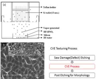
(8) 8. M. Ju et al. / Current Photovoltaic Research 6(1) 1-11 (2018). 3.2.4 Metal Assisted Chemical Etching (MACE). chemicals. At first, this method was studied to make PS (Porous. MACE is wet based etching technique like electrochemical. Silicon) structures43). The first released CVE device structure. etching. It is a catalyst etching where metal particles are. was observed in 2002. By placing silicon substrate on top cover,. involved in transferring of electrons that are needed for. air layer exists between the solution and silicon substrate, and. chemical reaction. In 1997, silicon etching using Al metal was. mixed acid solution is placed in a sealed container. The solution. tested. Then various metals like Ag, Au and Pt were deposited. is vaporized by heat bath and silicon substrate is etched by. on silicon using sputtering process and provided an opportunity. saturated acid vapor44). It is relatively simple and its cost is low.. to develop MACE process technology39). The mechanism of. However, it is not suitable for mass production of nano texturing. MACE is that oxidation-reduction of metal particles is repeated. for full-scale or large area etching due to its structural problem.. in silicon etching solution mixed with HF and HNO3 or HF and. For mass production, a simple nano texturing CVE device. H2O2, promoting etching of silicon surface and is as shown in. was developed in 2008 as seen in Fig. 20. Low cost CVE process. Fig. 19(a). The change of chemical etching rate by metal particle. was made possible to apply to mc-silicon solar cells45).. causes localized etching shape as seen in Fig. 19(c), (d) and (e).. The vapor generation for nano texturing can be done in two. Using this property, nanoscale structure can be formed on the. different ways. The first method is generating the required heat. surface.. energy with HF and HNO3 mixture and silicon. The ratio of HF. Recently applied MACE texturing is electroless plating using. and HNO3 mixed solution, induces a vigorous reaction with the. AgNO3. Ag metal particle is formed on the silicon wafer surface. added Si with large amount of heat and gas. The etching gas. 41). and chemical etching is proceeded . MACE texturing begins with removing saw damages from raw silicon wafer by acid etching as seen in Fig. 19. Etching process is carried out after forming silver particles by electroless plating using AgNO3, or AgNO3 is mixed with etching solution and formation of silver particle and etching occur at the same time42). When the etching is complete, silver particles remaining on silicon wafer surface is removed using HNO3 solution. Finally, post etching is carried out to control the nano structure morphology40). MACE texturing is wet based etching process and its cost is relatively low compared to other nano texturing process. However, the cost of chemicals used in MACE texturing is relatively high and the texturing process itself is complicated. The wet based nano texturing technology is similar to present conventional process. Fig. 20. Chemical Vapor Etching device used for the nano texturing process.. and could be next generation conventional process for mc-silicon solar cell market. 3.2.5 Chemical Vapor Etching (CVD). CVE is a method of etching silicon wafers physicochemically by vaporization of mixed solution of HF and HNO3, acid. Fig. 19. Metal Assisted Chemical Etching texturing process.. Fig. 21. Chemical Vapor Etching process used with external heating source..
(9) M. Ju et al. / Current Photovoltaic Research 6(1) 1-11 (2018). vaporized by the added silicon induce a heat reaction on the. 9. Acknowledgments. exposed silicon wafer and a nano structured textured surface was formed. In the second method an external heat source is used for the vapor generation and is depicted in Fig. 21. The etching gas fills the interior of the CVE device and excess gas is vented to the gap of upper cover and lower vessel. This work was supported by the Korea Institute of Energy Technology Evaluation and Planning (KETEP) and the Ministry of Trade, Industry & Energy (MOTIE) of the Republic of Korea (20163010012230).. holder maintaining the gas density and the pressure inside the device uniformly. CVE texturing is finalized by post etching for controlling the morphology of nano structures. Texturing by CVE process is simpler and less costly compared to RIE, ADE and MACE processes. It can be carried. References 1. X. Gu, X. Yun, K. Guo, L. Chen, D. Wang, D. Yang, “Seed-assisted cast quasi-single crystalline silicon for photovoltaic appli-. out in batch form and its potential as next generation conventional. cation: Towards high efficiency and low cost silicon solar. process for mass production of mc-silicon solar cells is very. cells”, Solar Energy Materials & Solar Cells, Vol. 101, pp. 95-101, 2012.. high.. 2. C. Park, J. Cho, Y. Lee, J. Park, M. Ju, Y-J Lee, J Yi, “Technology. 4. Conclusion. trends and prospects of silicon solar cells”, Current Photovoltaic research, Vol. 1, No. 1, pp. 11-16, 2013. 3. Fraunhofer Institute for Solar Energy Systems, ISE, “Photovoltaics. The mc-silicon solar cells take up a certain part of photovoltaic market despite of low efficiency compared to single crystalline silicon solar cells due to competitive production costs. However, the development of next generation technology, diamond wire sawing which reduces the production cost of single crystalline. Report”, 2015. 4. V. Benda, “Crystalline silicon cells and modules in present photovoltaics”, Journal of Engineering Science and Technology Review, Vol. 7, No. 2, pp. 7-15. 2014. 5. PHOTON Consulting, LLC, “The true cost of solar power, how low can you go?”, 2010.. silicon solar cells causes optical loss for existing multi-silicon. 6. A. Goodrich, P. Hacke, Q. Wang, B. Sopori, R. Margolis, T. L.. solar cells acting as an obstacle to production implementation.. James, M. Woodhouse, “A wafer-based monocrystalline sili-. In this paper, the mechanism of general texturing process based. con photovoltaics road map: Utilizing known technology im-. on HF and HNO3 is analyzed to see the limit of multi-silicon solar cell surface structures and the root cause of optical loss of diamond wire sawed wafers. The next generation texturing processes are investigated. The features that the next generation texturing processes should have are: a) an unique texturing process irrespective of the crystal orientation of silicon wafer, b) the process should be simple and low cost and c) the solar cell efficiency should be high through the reduction of reflectivity.. provement opportunities for further reductions in manufacturing costs”, Solar Energy Materials and Solar Cells Vol. 114, pp. 110-135, 2013. 7. H. Wu, “Wire sawing technology: A state-of-the-art review”, Precision engineering, Vol. 43, pp. 1-9, 2016. 8. F. Cao, K. Chen, J. Zhang, X. Ye, J. Li, S. Zou, X. Su, “Next-generation multi-crystalline silicon solar cells: Diamond-wire sawing, nano-texture and high efficiency”, Solar Energy Materials and Solar cells, Vol. 141, pp. 132-138, 2015. 9. B. Meinel, T. Koschwitz, J. Acker, “Textural development of SiC and diamond wire sawed sc-silicon wafer”, Energy Procedia, Vol. 27, pp. 330-336, 2012.. The technologies in close proximity to these items seem to be. 10. M. Steinert, J. Acker, A. Henbge, K. Wetzig, “Experimental. Atmospheric pressure Dry chemical Etching (ADE), Chemical. studies on the mechanism of wet chemical etching of silicon in. Vapor Etching (CVE) and Metal Assisted Chemical Etching (MACE). The leap of low-cost, high-efficiency multi-silicon. HF/HNO3 mixtures”, Journal of The Electrochemical Society, Vol. 152 No. 12, pp. C843-C850, 2005. 11. M. Steinert, J. Acker, M. Krause, S. Oswald, K. Wetzig, “Reactive. solar cells is expected through the application of these tech-. Species Generated during Wet Chemical Etching of Silicon in. nologies.. HF/HNO3 Mixtures”, Journal of Physical Chemistry B, Vol. 110, pp. 11377-11382, 2006. 12. D. J. Monk, D. S. Soane, R. T. Howe, “A review of the chemical reaction mechanism and kinetics for hydrofluoric acid etching of silicon dioxide for surface micromachining applica-.
(10) 10. M. Ju et al. / Current Photovoltaic Research 6(1) 1-11 (2018). tions,”, Thin Solid Films, Vol. 232, pp. 1-12, 1993.. 2011.. 13. G. W. Trucks, K. Raghavachari, G. S. Higashi, Y. J. Chabal,. 27. H. Savin, P. Repo, G. Gastrow, P. Ortega, E. Calle, M. Garín,. “Mechanism of HF etching of silicon surfaces: A theoretical un-. R. Alcubilla, “Black silicon solar cells with interdigitated back-. derstanding of hydrogen passivation”, Physical Review Letters,. contacts achieve 22.1% efficiency”, Nature Nanotechnology,. Vol. 65, No. 4, pp. 504-507.. Vol. 10, pp. 624-629, 2015.. 14. H. Robbins, B. Schwartz, “Chemical etching of silicon”,. 28. K. Fukui, Y. Inomata, K. Shirasawa, “Surface texturing using. Journal of the electrochemical society, Vol. 106, No. 6, pp. 505-. reactive ion etching for multicrystalline silicon solar cells”,. 508, 1959.. Photovoltaic Specialists Conference, 1997., Conference Record. 15. H. Robbins, B. Schwartz, “Chemical etching of silicon”, Journal of the electrochemical society, Vol. 107, No. 2, pp. 108-111.. of the Twenty-Sixth IEEE Date Sept. 29 1997-Oct. 3 1997. 29. M. S. Yun, D. H. Hyun, B. J. Jin, J. Y. Choi, J. S. Kim, H. D.. 16. K. Chen, Y. Liu, X. Wang, L. Zhang, X. Su, “Novel texturing. Kang, J. Yi, G. C. Kwon, “Study of low reflectance and RF fre-. process for diamond-wire-sawn single-crystalline silicon solar. quency by rie surface texture process in multi crystal silicon so-. cell”, Solar Energy Materials and Solar Cells, Vol. 133, pp.. lar cells”, Journal of the Korean Vacuum Society Vol. 19, pp.. 148-155, 2015.. 114-120, 2010.. 17. J. Zhao, A. Wang, F. Ferrazza, M. A. Green, “19.8% efficient. 30. W. Chen, H. Lin, F. C. Hong, “Improvement of conversion effi. ‘‘honeycomb’’ textured multicrystalline and 24.4% mono-. ciency of multi-crystalline silicon solar cells using reactive ion. crystalline silicon solar cells”, Applied Physics Letters, Vol. 73,. etching with surface pre-etching”, Thin Solid Films Vol. 597,. No. 14, pp. 1991-1993, 1998.. pp. 50-56, 2015.. 18. A. Volk, N. Tucher, J. Seiffe, H. Hauser, M. Zimmer, B. Blasi,. 31. P. Feng, G. Liu, W. Wu, Y. Shi, Q. Wan, “Improving the blue. M. Hofmann, J. Rentsch, “Honeycomb structure on multi-. response and efficiency of multicrystalline silicon solar cells by. crystalline silicon Al-BSF solar cell with 17.8% efficiency”, Ieee. surface nanotexturing”, IEEE Electron Device Letters, Vol. 37,. Journal Of Photovoltaics, Vol. 5, No. 4, pp. 1027-1033, 2015.. pp. 306-309, 2016.. 19. C. Gerhards, C. Marckmann, R. Tolle, M. Spiegel, P. Fath, G.. 32. B. Kafle, J. Seiffe, M. Hofmann, L. Clochard, E. Duffy, J.. Willeke, E. Bucher, J. Creager, S. Narayanan, “Mechanically. Rentsch, “Nanostructuring of c-Si surface by F2-based atmos-. V-textured low cost multicrystalline silicon solar cells with a. pheric pressure dry texturing process applications and materials. novel printing metallization”, Photovoltaic Specialists Conference,. science”, Phys. Status Solidi A, Vol. 212, No. 2, pp. 307-311,. 1997., Conference Record of the Twenty-Sixth IEEE Date Sept. 29 1997-Oct. 3 1997.. 2015. 33. B. Kafle, A. Mannan, T. Freund, L. Clochard, E. Duffy, J.. 20. M. Abbott, J. Cotter, “Optical and electrical properties of laser. Rentsch, M. Hofmann, Ralf Preu, “Nanotextured multicrystal-. texturing for high effciency solar cells”, Progress in Photovoltaics:. line Al-BSF solar cells reaching 18% conversion efficiency us-. Research and Applications, Vol. 14, pp. 225-235, 2006.. ing industrially viable solar cell processes”, Phys. Status Solidi. 21. L. A. Dobrazanski, A. Drygala, “Surface texturing of multi-. RRL, Vol. 9, No. 8, pp. 448-452, 2015.. crystalline silicon solar cells”, Journal of Achievements in. 34. Michael J. Sailor, Porous Silicon in Practice: Preparation,. Materials and Manufacturing engineering, Vol. 31, pp. 77-82,. Characterization and Applications, 2012 Wiley-VCH Verlag. 2008.. GmbH & Co. KGaA.. 22. P. Choi, J. Kim, M. Kim, J. Cho, D. Baek, S. Kim, B. Choi,. 35. R. R. Bilyalov, R. LuKdemann, W. Wettling, L. Stalmans, J.. “Enhanced efficiency of multicrystalline silicon solar cells. Poortmans, J. Nijs, L. Schirone, G. Sotgiu, S. Strehlke, C.. made via UV laser texturing”, Journal of the Korean Physical. Levy-Clement, “Multicrystalline silicon solar cells with porous. Society, Vol. 67, No. 6, pp. 991-994, 2015.. silicon emitter”, Solar Energy Materials & Solar Cells, Vol. 60,. 23. E. Lohmuller, B. Thadigsmann, J. Bartsch, C. Harmel, J. Specht, A. Wolf, F. Clement, M. Horteis, D. Biro, “Advanced metallization of rear surface passivated metal wrap through silicon solar cells”, Energy Procedia, Vol. 8, pp. 546-551, 2011. 24. W. Neu, A. Kress, W. Jooss, P. Fath, E. Bucher, “Low-cost. pp. 391-420, 2000. 36. C. Pacholski, “Photonic crystal sensors based on porous silicon”, Sensors, Vol. 13, pp. 4694-4713, 2013. 37. B. Bhushan (ed.), Encyclopedia of Nanotechnology, DOI 10.1007/978-90-481-9751-4.. multicrystalline back-contact silicon solar cells with screen. 38. V. Y. Yerokhov, R. Hezel, M. Lipinski, R. Ciach, H. Nagel, A.. printed metallization”, Solar Energy Materials & Solar Cells. Mylyanych, P. Panek, “Cost-effective methods of texturing for. Vol.74, pp. 139-146, 2002.. silicon solar cells”, Solar Energy Materials & Solar Cells Vol.. 25. M. M. Hilali, J. M. Gee, P. Hacke, “Bow in screen-printed back-contact industrial silicon solar cells”, Solar Energy Materials & Solar Cells, Vol. 91, pp. 1228-1233, 2007. 26. S. Gatz, K. Bothe, J. Müller, T. Dullweber, R. Brendel, “Analysis. 72, pp. 291-298, 2002. 39. Z. Huang, N. Geyer, P. Werner, J. Boor, U. Gösele, “MetalAssisted Chemical Etching of Silicon: A Review”, Advanced Materials, Vol. 23, pp. 285-308, 2011.. of local Al-doped back surface fields for high efficiency. 40. J. Oh, H. Yuan, H. M. Branz, “An 18.2%-efficient black-silicon. screen-printed solar cells”, Energy Procedia Vol. 8, pp. 318-323,. solar cell achieved through control of carrier recombination in.
(11) M. Ju et al. / Current Photovoltaic Research 6(1) 1-11 (2018). 11. nanostructures”, Nature Nanotechnology, Vol. 7, pp. 743-748,. R. Bennaceur, “Application of the chemical vapor-etching in-. 2012.. polycrystalline silicon solar cells”, Applied Surface Science. 41. S. K. Srivastava, P. Singh, M. Yameen, P. Prathap, C. M. S.. Vol. 252, pp. 488-493, 2005.. Rauthan, Vandana, P. K. Singh, “Antireflective ultra-fast nano-. 44. M. Saadoun, N. Mliki, H. Kaabi, K. Daoudi, B. Bessaıs, H.. scale texturing for efficient multi-crystalline silicon solar cells”,. Ezzaouia, R. Bennaceur, “Vapour-etching-based porous sili-. Solar Energy Vol. 115, pp. 656-666, 2015.. con: a new approach”, Thin Solid Films, Vol. 405, pp. 29-34,. 42. Z. G. Huang, X. X. Lin, Y. Zeng, S. H. Zhong, X. M. Song, C.. 2002.. Liu, X. Yuan, W. Z. Shen, “One-step-MACE nano/micro-. 45. M. Ju, M. Gunasekaran, K. Kim, K. Han, I. Moon, K. Lee, S.. structures for high-efficient large-size multicrystalline Si solar. Han, T. Kwon, D. Kyung, J. Yi, “A new vapor texturing meth-. cells”, Solar Energy Materials & Solar Cells, Vol. 143, pp.. od for multicrystalline silicon solar cell applications”, Materials. 302-310, 2015.. Science and Engineering B, Vol. 153, pp. 66-69, 2008.. 43. M. B. Rabha, M. Saadoun, M. F. Boujmil, B. Bessaı, H. Ezzaouia,.
(12)
수치
+4
관련 문서
