The study of shape of electrodes and I-V characteristics for Ultraviolet LED
Nguyen Huu Trung
★*, Vu The Dang
**and Nguyen Van Hieu
*Abstract
About functional parameters of a LED / UVLED (Light Emitting Diode/Ultra Violet LED), one of the most important parameters is the I-V characteristic. By researching factors affect to the I-V characteristic of uvled, we found that beside of the structure of the device itself, there is the influence of the electrode materials, electrode shapes, the process of wiring and packaging. In this work, we want to improve the performance of UVLED to find out the optimal mask design principles. The study is based on theoretical mathematical models, as well as the use of simulation software tool Comsol. From all results obtained, the team has improved mask design to manufacture electrodes for GaN-based UVLED. Electrode masks are designed by three softwares, which are Intellisuite, Klayout and AutoCad. Intellisuite masks would be used in fabrication simulation while Klayout and AutoCad are used to fabricate electrodes in experiments. As well as, we silmulated the structure of an uvled 355nm emission wavelength by TCAD software, in order to compare with uvled sample that has the same emission wavelength.
Keywords: shape of electrodes, uvled, mask process, I-V curves, Klayout.
.*Dept. of Physics and Electronic Engineering, University of Science, VNU.HCM City, Vietnam.
**Semiconductors Technology, Saigon Hi-Tech Park Labs, HCM City, Vietnam.
★ Corresponding author: Nguyen Huu Trung, [email protected].
Office Tel: ++84.8.38.300595.
※ Acknowledgment: This research is funded by The Department of Science and Technology
HoChiMinh City (DOST.HCM) from
08/2010-08/2013.
Manuscript received May. 13.2013; revised July. 08.
2013; accepted July. 08. 2013
Ⅰ. Introduction
Electrode is an indispensable component in the electronics or microelectronics devices. Especially in the micro-electronic devices, the role of a good or bad electrode has significant effects to the operation of those devices. Devices with non-standard electrodes may not work with good agreements with the original design. This can reduce life time and
performance of devices. For example, in light-emitting components such as LED or UVLED, electrode is a important component that decides emitting performance and I-V characteristic.
About functional parameters of uvled, one of the most important parameters is I-V characteristic. By researching on factors affect to the I-V characteristic of UVLED, we found that not only structure of the components, but also electrode materials, electrode shapes, wiring and packaging process affect to function of devices.
To solve above issues, we has focused on building models to figure out design principles for its electrode shape. We also propose steps in an electrode fabrication process for them on both simulations and experiments.
The content presented in this report:
Theoretical model for ideal electrode shapes and simulate the resistance of the electrode shapes;
design of masks for UVLED electrodes and electrodes fabrication processes UVLED; and investigation of the I-V characteristic and
wavelength of UVLED
Ⅱ. Experimental Methods
The mathematical tools and software Comsol were used to survey the specific electrode shapes, in order to find out the optimal electrode shape. Then, the mask for electrode fabrication process were designed by the softwares of Intellimask, Klayout, AutoCAD.
The fabrication process of LED structures were studied through software Intellisuite. Finally, TCAD software is used to simulate the I-V curve of the LED to compare with the measring uvled samples made in lab for Semiconductor Technology, Saigon Hi-Tech Park, HoChiMinh, Vietnam.
Ⅲ. Experimental Results
3.1. Design electrode shapes
Electrode mask design for UVLED is a very important step in the entire process of fabrication.
Electrodes are manufactured to meet small resistance requires, in order to avoid large power loss and heat [3],[4]. On the other hand, the shape of the electrode has a huge impact on emitting performance, the I-V characteristics, ... of UVLED devices. Therefore, a good electrode which satisfies the criterias as mentioned plays a very important role in improving the performance and life time of devices as well.
Mathematic apporach
We assume the current in LED is uniform with current density, J. When Jisthe current density and
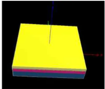
Fig 2. Electrode structure in the LED model.
Vactive is the voltage at the active layers, the voltage applied to both ends of the current road A, VroadA, in Fig.2 (a) can be represented as [1]
VroadA= J.(ρ p-electrode .tp-electrode +ρ p .tp+ρ n- electrode
.tn-electrode +ρ n .tn)+Va .
In which:
J : the uniform current density in the LED structure (A/m2).
ρp-electrode:the resistivity of the electrode p.
tp-electrode:thickness of the electrode p.
ρ p:the resistivity of the p-GaN layer.
tp:the thickness of the p-GaN layer.
ρ n-electrode : the electrode resistivity of electrode n . tn-electrode:thickness of the electrode n.
ρ n: the resistivity of the n-GaN layer.
tn:the thickness of the n-GaN layer.
Va:the voltage in the active layer.
Similarly, the voltage at the second road B is calculated by the model:
VroadB=J.(ρ p-electrode .tp-electrode +ρ p .tp+ρ n- electrode .tn-electrode +ρ n .l)+Va
In which, lis the horizontal distance in the n-GaN layer where current moves:
Fig 3. Electrode structure in the LED model while reducing distance l.
Because the voltage at the two electrodes of both A and B road are equal, then:
VroadA=VroadB (*) (*) equation can be infered:
J. ρ n (tn -l)=0
Because tn<<l,(*)becomes -J. ρ nl =0 or J.ρnl=constant(**)
From equation (**) we see that it is possible to adjust the current in the LED by reducing the
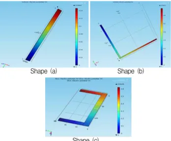
Shape (a) Shape (b)
Shape (c)
Shape Resistance, R(Ω)
Au layer Ni layer Al layer
(a) 0.5044 1.6667 0.6479
(b) 0.4946 1.6343 0.6353
(c) 0.4847 1.6014 0.6226
resistivity of the n-GaN or decrease parameter l. To reduce the resistivity ρn, we have to increase the doping concentration in the n-GaN. But this method has a disadvantage is that the doping concentration of GaN can only be adjusted within a certain limitation [1]. When we dope into nGaN too much, it will damage the lattice structure of GaN. Thus, the best way is to reduce thevalue of parameter l.
Resistence of electrodes
In addition to the parameters affect to a density of LED that has been analyzed in the section above, there is another factor also impacts on the performance of the LED . That is a resistance of the electrode block. Electrodes are manufactured to meet small resistance criteria, in order to avoid large power loss and heat. The goal of this section simulation is using Comsol tool to calculate resistance values of different electrode shapes.
The formular of resistance of the conductive material is: R=ρ.l/S
With: ρ: resistivity, l: length of material, S: the area of a cross section of the current passing through.
When we survey the influence of electrode shapes to the resistance values, the electrode shapes must meet the criteria is that the cross section and the total length must be the same. This means that in theory, the resistance value would be equal because of the same input parameters. But in reality, because of influence of the shape, the resistance value is different indeed.
Silmulation results
This phenomenon can be explained: although in theory, all three shapes have the same length l and cross-sectional area S, but in the shape of the electrode that has segments, the current would not go the entire distance, but it just focuses at an angle. This causes that a current density at that corner increases, and the distance of current is in fact shorter than it does in theory. The more segments are there in shapes, the smaller resistor is.
The results are shown with the same rule when we simulate with other materials as Ni, Au and Al, shown in Table 1.
Fig 4. Simulation results of electrode resistence: (a), the resistance of the sample with the largest value, (b), the resistance decreases as the electrode shape have one segment and (c), electrode 2 segments.
Table 1. Simulation results for resistance of electrodes in each material and each shape.
The results showed that the material Gold (Au) have the lowest resistance, which followed by aluminum (Al) and nickel (Ni). For each material, the resistance value also showed the same rule. Therefore, we figure out the solution for ideal resistance shape:
. The space between the positive / negative electrode must be short, but not too short to avoid parasitic current.
. Density of metal electrode on surface must be high. Electrode shape should have many branches and uniform.
. There are many branches of electrode to reduce the value of the resistance.
3.2. Mask design for electrodes
The mask would be designed by the three software Intellimask, Klayout and AutoCad. Each set includes 2 masks. Those would be used in fabrication
(a) (b)
process which would be presented and simulated in the next section. The mask is designed with 2 inch standard wafer.
Inparticular,version Intellimask will be used to simulate the manufacturing process. Two versions Klayout and AutoCad will be used to produce masks that fabricate electrodes.
Figure 5. Electrode structure in the LED model while reducing the distance of l: (a), using Klayout design and (b), AutoCAD design.
3.3. Electrode fabrication process for UVLED Next, we studied the fabrication process UVLED consists of six main steps as shown below. Two masks are used to generate the P and N semiconductor layer on EPI wafer and shaped the electrodes. We conducted simulation to support manufacturing in the clean room of the Saigon Hi-tech Park, Hochiminh City.[2]
Step 1: Manipulation on UVLED EPI wafer and photoresist coating
Fig 6. Cleaning wafer with equipment SRD Avengers Basic 8.
Organic contamination on the wafer is cleaned with H2SO4 and DI water, dried with N2.
Step 2: Photolithography process on EPI wafer with mask 1, including:
Fig 7. Maniulation with mask 1.
- Coating primer on the wafer surface, using a spin coating.
-Coating photoresist on the surface of the wafer.
-Heating wafer on hotplate at a temperature of 11500C in the 50s.[2]
-Photolithography with mask 1, using a Mask Aligner MJB4
-Removing the photoresist with AZ726 MIF solution.
Then, heatting wafer on a hotplate at a temperature of 12500C for 60s. [2]
Step 3: Wet etching the GaN layers.
Figure 8. Etched GaN layers with NaOH solution ratio 6: 1, cleaned with DI water and N2 gas blowing.
Step 4: Sputtering Ni (500nm) / Al (1,000 Nm) We used the DC magnetron sputtering, ACS-4000-C4. Gas is used is argon. Equipment used two 200V DC power supply and RF 60 Hz with 4 cathode.
Fig 9. Sputtering Ni films (500nm) / Al (1,000 nm)
Step 5: The process of photolithography with mask 2 Includingtwo stages:
- Coating (photoresist) on the wafer surface, turning light and heat.
-Lithography process with mask 2, using a Mask Aligner MJB4.
Step 6: Etching the layers of Al and Ni.
Fig 10. Etching the layers of Al and Ni.
- Aluminum is etched by a mixed solution includes:
phosphoric acid (H3PO4),nitric acid (HNO3),acetic acid (CH3COOH),and water (H2O).In particular, nitric acid turn Al into Al2O3, then aluminum oxide (Al2O3)isdissolvedwith phosphoric acid. Acetic acid and water acts as a solvent to dissolve.
- Nickel and Aluminum are etched in a mixed solution includes: acid and phosphoric acid (H3PO4),nitric acid (HNO3),acetic acid (CH3COOH),and water (H2O).
Result: We are successful in fabricate masks for UVLED electrode. From those masks, we continued to fabricate electrodes for UVLED structure. Here are some images of electrodes we fabricated:
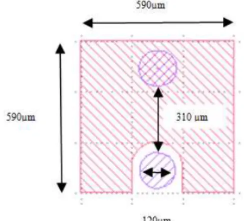
Figure 11. Electrodes for UVLED 355nm and 320nm Dimensions of electrode for 355nm UVLED
One die of UVLED is 595 µm x 595µm, as shown in
fig 12. In which, width of each branch of electrode iss 20 µm. Gap between anode and cathode is also 20 µm.
Fig 12. Dimensions of optimal electrode.
One die of UVLED is 595 µm x 595µm, as shown in fig 12. In which, width of each branch of electrode is 20 µm. Gap between anode and cathode is also 20 µm. Distance between anode and cathode is about 115µm.
Fig 13. Dimensions of conventional electrode.
In comparsion to conventional UVLED electrodes, the distance between cathode and anode is about 310 µm. We can see the distance in optimal electrode is two times shorter than the conventional electrode.
3.4. The I-Vchracteristics for UVLED
We conducted simulation of I-V characteristics of
Material Epilayer Thickness (nm)
Doping (cm-3)
Mobility (cm/V.s)
GaN p-contact 100 1020 10
Al0.2GaN p-emitter 100 1020 10
GaN 3 MQW 3 / 200
Al0.2GaN 2 barriers 7 / 100
Al0.2GaN n-emitter 100 2x10¹⁸ 100
GaN n-contact 300 2x10¹⁸ 100
GaN-based UVLED with structure:
Table 2. Structural parameters in UVLED 355nm.
Fig 14. Electrode shape of 355nm LED with dimensions determined.
We write program code 355nm structure by TCAD software to silmulate I-V characteristic and emission wavelength.
We also conducted some experiments to revise the I-V charateristic and emission wavelength of 355nm UVLED to compare with the results of simulation.
Fig 15. I-V characteristics of LED with the horizontal axis is voltage applied and the vertical axis is anode current. Polarizing voltage is about 3.0 (V)
When compared the results with the I-V characteristic of 355nm UVLED between the simulation (fig.15) and experiment (fig.18), we found
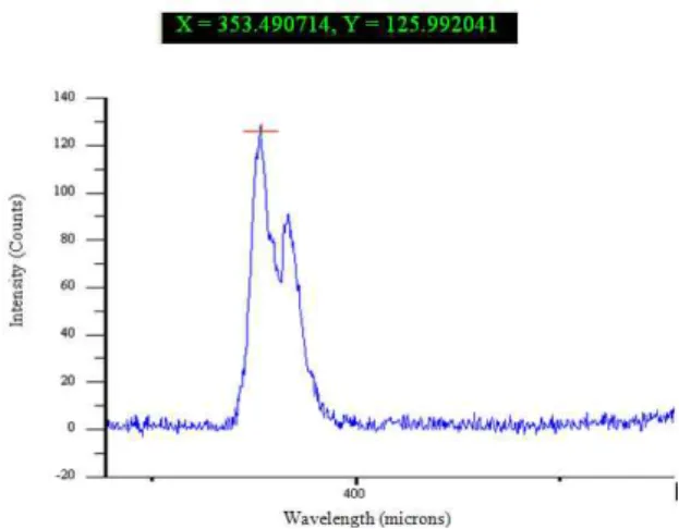
Fig 16. UVLED’s peak emission wavelength is about 355nm by horizontal axis, and vertical axis is emission intensity.
Fig 17. Emission of 355nm UVLED.
Fig 18. The I-V characteristics of LED 355nm polarized at 3.0 (V).
very similar results in shape of I-V curves.
However, the difference is that the simulation curveincreases slowly. Means while, in the experiment, the curve increased vertically and reach a saturated state sooner. The difference may come from the effects of optimal electrode to the I-V curve of UVLED. About the comparison between
Fig 19. Emission wavelength of 355nm UVLED in experiment.
emission wavelength of simulation and experiment, we saw a small difference. While the simulation result is 355nm, the experiment is 353.5 nm, but this gap can be ignored. The results will provide the parameters for us to take steps to make electrodes for UV LED in SHTP in next times.
Ⅴ. Conclusion
In this paper, authors have found principles to design optimal electrode shapes using two methods is to build theoretical model calculation and simulation resistor by software Comsol. Using the results obtained in this section, the author completed mask design with 3 softwares, which is Intellimask, Klayout and AutoCad. Particularly, Intellimask is used to simulate the manufacturing process and the two other are used to fabricate in experiments.
Moreover, through simulation, the authors set out the a UVLED emission structure in the light of 355nm, as well as the I-V characteristic survey of UVLED samples.
The study of UVLED structures with multiquantun wells (MQWs) already reported by our group via the means of SiLENSE with many usefl data for our next fabrication [5,7,8]. Moreover, the design and fabrication for capacitive pressure sensor (CPS) for high temperature application also studied in fabrication process [6] via the co-operation research group in Japan. Therefore, the study of shape of electrodes and I-V characteristics for Ultraviolet LED
will be useful data for our next step of the fabrication process of uvled in SHTP.
Acknowledgment
This work is supported in part by the Grant-in-Aid for Scientific Research (78/HD-SKHCN, B2011-18-33) from the government of HCMC and Vietnam National University HCMC.
Author specially thank our colleagues in Ritsumeikan University (Japan) for SiLENSe software. We also thanks colleagues in lab for semicondoctors technologies-SHTP, Dr. Phan Bach Thang (Lab for Material Advanced Technology, HCMUS) for semiconducting equipment, Dr. Ho Thanh Huy and Prof. T. Ishida (OPU, Japan) for the useful assistant of photography process.
The authors also thank the technical committee of IKEEE for fruitful comments and suggestion which help to improve the quality of this paper.
References
[1] Joo Sun Yun, Sung Min Hwang, Jong In Shim,Department of Electrical and Computer Engineering, Hanyang University, 1271 Sa-1 dong, Ansan,Kyunggi-do 425-791, Korea
“Current Spreading Analysis in Vertical Electrode GaN-based Blue LEDs”, Proc. of SPIE Vol. 6841 68410L-2, pp. 3.
[2] Nguyen Viet Hung and Nguyen Viet The: “Design, manufacture electrode layer for Schottky diode with high breakdown voltage and leakage current very little for flow control applications in the power storage device, electric cars”, Research project in SHTP, HCMC, pp. 64-66 (private commnication).
[3] H. S. Kim, J. M. Lee, C. Huh, S. W. Kim, D. J.
Kim, S. J. Park, and H. S. Hwang, “Modeling of a GaN-based lightemitting diode for uniform current spreading,” Appl. Phys. Lett., Vol. 77, No. 12, pp.
1903-1904, 2000.
[4] H. S. Kim, S. J. Park, and H. S. Hwang, “Lateral current transport path, a model for GaN-based light-emitting.
diodes: Applications to practical device designs,” Appl.
Phys. Lett., Vol. 81, No. 7, pp. 1326-1828, 2002.
[5]. Nguyen Van Hieu and Hynh Huu Trung, The Study of Doping Concentration in ALyGA1-y Block Layer Based on Multi Quantum Well of 313m LED, Journal of Emerging Trends in Engineering and applied sciences, Vol2, No.6, p1054-1058 (Dec.,2011).
[6]. Tran Le Thien Thuy, S. Tanaka, M. Essashi and Nguyen Van Hieuu, The Capacitive Pressure Sensor for High Temperature Application: Design and Fabrication, Journal of Emerging Trends in Engineering and applied sciences, Vol2, No.6, p576-580 (Dec.,2011).
[7].Bui Van Quang, Huynh Hoang Trung and Nguyen Van Hieu: The study of number and thickness of Multi quantum well based on AlGaN UVLED,the 3rd International Workshop on Nanotechnologies and Applications, IWNA2011 [VNU-HCMC& MINATEC (France)], NMD-172-P ,p.792 (Nov., 2011).
[8].Huynh Hoang Trung and Nguyen Van Hieu:
Wavelength dependent of doping concentration in AlyGa1-yN block layer for MQW UVLED, the 3rd International Workshop on Nanotechnologies and Applications, IWNA2011 [VNU-HCMC& MINATEC (France)], NFT-030-P ,p.519 (Nov., 2011).
BIOGRAPHY
NguyenHuuTrung
2009.9. University of Science (VNU.HCM), Hochiminh City, Dept. of Electronic Engineering (Bachelor).
2011.09-now. Co-worker, Semiconductors Technology, Saigon Hi-Tech Park Labs,HCM City, Vietnam.
2013. University of Science (VNU.HCM), Hochiminh City, Dept. of Electronic Engineering (Master).
2009.9-now. University of Science (VNU.HCM), Hochiminh City, Dept. of Physics and Electronic Engineering: Teaching assistant, researcher,
assistant lecturer.
<Research Interests> MEMS, Semiconductors Devices, Microelectronics,
VuTheDang
2007.9. Ho Chi Minh university technical of education, Electronic Engineering (Engineer).
2010.10. Ho Chi Minh university technical of education, Electronic Engineering (Master of
Engineering).
2008.10-2011.8. Southern technology and agro - Forestry Vocational College (Lecturer).
2011. 9-now. Binh Duong Economic and Technology University (deputy head, dept. of electronics).
2010. 5- now. Co-worker, Semiconductors Technology, Saigon Hi-Tech Park Labs,HCM City, Vietnam.
<Research Interests> Semiconductors Devices, Microprocessor, Electronic Engineering.
NguyenVanHieu
1994.9. University of Hochiminh City, Dept. of Electronic Engineering ( BS).
1996.9. Hanoi Foreign Language, Dept. of English (Bachelor) 2000. 6. University of Science (VNU.HCM), Hochiminh City, Dept. of Electronic Engineering (Master).
2007. 3. Osaka University, Japan, Dept. of Physics, Electronic and Magnetic Devices (Ph.D).
2010. 3. Inviting Researcher, Ritsumeikan University, Japan, Dept. of Semiconductors and photonic Devices .
2011- now. Inviting Researcher, Semiconductors Technology, Saigon Hi-Tech Park Labs,HCM City, Vietnam.
2007.4- now: University of Science (VNU.HCM), Dept. of Physics and Electronic Engineering, senior lecturer, associate professor, head of dept.
<Research Interests> Semiconductors and photonic Devices, Microelectronics, MEMS, Electronic Engineering.