논문 2016-53-9-9
다중/집중리더 환경에 적합한 다중 직교 부반송파 변조 기반 고속 UHF RFID 시스템
( Multiple Orthogonal Subcarrier Modulation based High-Speed UHF RFID System for Multiple-/Dense-Interrogator Environments )
박 형 철*
( Hyung Chul Park
ⓒ)
요 약
본 논문에서는 다중 직교 부반송파 변조 기반의 새로운 UHF RFID 통신 시스템을 제안한다. 태그 송신-리더 수신 통신에 서는 4 부반송파를 이용하여 1.6 Mbps까지 전송속도를 향상시킬 수 있다. 회로의 복잡도 증가를 억제하면서도 전송 속도를 향 상시키기 위해서, 태그는 부반송파로서 구형파를 사용하고 각 부반송파는 각각의 부하변조기를 이용한다. 다중 직교 부반송파 기반의 변조 방식을 사용하였기 때문에 제안한 통신 방식은 기존의 UHF 대역 RFID 규격을 만족한다. 리더는 OFDM 복조기 를 사용한다. 태그가 리더의 CW 반송파를 역산란하므로 리더 복조기에는 반송파 주파수 오프셋 보정회로는 필요하지 않다.
실험에서는 개발 시스템은 10.8 dB의 잡음 밀도당 비트에너지 비에서 10-5의 비트오율 성능을 가짐을 보인다.
Abstract
This paper presents a novel multiple orthogonal subcarrier modulation based UHF band RFID communication system. In tag-to-reader communication, the demonstration system can deliver 1.6 Mbps through four subcarriers. To improve data rate while suppressing increase in circuit complexity, tag employs square-waves as the subcarriers and uses individual load modulators for each subcarrier. By using multiple orthogonal subcarrier based modulation, proposed communication system can be operated under existing UHF band RFID regulation. In reader, an OFDM demodulator is used. Since the tag backscatters the reader’s CW carrier, carrier frequency offset compensation is not necessary in reader demodulator.
Experimental results show that the demonstration system achieves a bit error rate of 10-5 at an Eb/N0 of 10.8 dB.
Keywords : UHF RFID, Passive tag, OFDM, Load modulation, FFT
* 정회원, 서울과학기술대학교 전자IT미디어공학과 (Dept. of Electronic and IT Media Engineering, Seoul National University of Science and Technology)
ⓒCorresponding Author (E-mail : [email protected])
※ 이 연구는 서울과학기술대학교 교내 학술연구비 지원으로 수행되었습니다.
Received ; April 5, 2016 Revised ; August 24, 2016 Accepted ; September 2, 2016
Ⅰ. Introduction
Passive radio frequency identification (RFID) is gaining a greater market share because passive RFID technology has advantages over barcodes, including
non-line of sight (NLOS) communication, increased data speed, and a longer read range.[1~10] In [1], [2], RFID technologies was introduced. In [4~7], [10], applications of UHF RFID were presented. In [3], [8],
[9], performance / function enhancement technologies for UHF RFID were presented. However, as passive RFID technology is used to read a large amount of data from a tag, an improvement in the data rate is required. In particular, aerospace companies require high-speed and high-performance passive RFID technology. In some previous studies, high data rate RFID technology has been studied.[11~14] In [11], an
impulse radio ultrawide bandwidth (IR-UWB) technology was used. The uplink (tag-reader) data rate is increased up to 1 Mbps. However, since an IR-UWB signal occupies several GHz, the spectrum efficiency is very low. In [12], a conventional inverse fast Fourier transform (IFFT)-based orthogonal frequency division multiplexing (OFDM) technology was used in a tag. In addition, conventional analog and RF circuits, such as a digital-to-analog converter (DAC), a frequency synthesizer, and a RF up converter, are used in the tag. Hence, the tag consumes more power and is very complex and expensive. In [13], it was shown that the uplink (tag-reader) data rate can be increased up to 5 Mbps using existing UHF RFID tag communication. In [14], a complex backscatter based quadrature phase-shift keying (QPSK) was used to improve spectrum efficiency. However, since the backscattered power is the same as that of existing UHF RFID tag, the signal-to-noise ratio (SNR) is degraded due to the reduced minimum constellation spacing. In addition, since the semi-passive RFID techniques is used in the developed system, battery is used for complex backscattering. This paper presents a multiple orthogonal subcarrier modulation based UHF band RFID communication system. In tag-to-reader communication, the demonstration system can deliver 1.6 Mbps through four subcarriers. For tag-to-reader communication, proposed system uses a multiple orthogonal subcarrier modulation to improve data rate while enabling the operation under existing UHF band RFID regulation. In the proposed system, square-waves are used instead of complex exponentials as the subcarriers. By using square- waves as the subcarriers and individual load modulators for each subcarrier, complexity of tag integrated circuit is almost the same as that of existing tag because DAC and memory for subcarrier are not necessary.
Ⅱ. Square-wave subcarrier OFDM
An OFDM signal can generally be written as [15]( ) ∑ ∑
∞( )
−∞
=
−
=
⎟⎟⎠
⎜⎜ ⎞
⎝
= ⎛
n 2 1 N
2 -N k
s s k
n,
s
s
nT - T t j2π k exp s t
s (1)
where sn,k denotes the symbol modulated by the k-th subcarrier during the symbol time of index n, Ts
represents the symbol duration, and Ns denotes the number of subcarriers. As shown in (1), it is worth noting that complex exponential functions are used for OFDM subcarriers. Using Euler's formula, a complex exponential is expressed in terms of the sine and cosine. Hence, DACs are necessary for OFDM transmission. However, passive RFID tags must not use DACs owing to a power limitation and cost constraint. This means that a complex exponential subcarrier-based OFDM technology cannot be used for passive RFID tags. In the proposed square-wave subcarrier-based OFDM technology, a square wave can be represented as
( ) ∑
∞( [ ( ) ] [ ( ) ] )
−∞
= − − − +
=
n
T 4 1 n t u T 4 1 - n t u t
p (2)
where T denotes the period of a square wave, and u(t) is the unit step function. In the proposed method, p(t) is used as the subcarriers, the same as complex exponential functions in (1). As shown in (2), the square wave represents a binary value (high or low).
When square waves with different frequencies are superposed, the resulting signal has multiple amplitudes such that DACs are necessary. If a DAC is used, DAC output controls the impedance of a load modulator. However, since the impedance is dependent on process or device, the signal quality may be degraded. To remove the DACs, each square-wave subcarrier signal uses its own load modulator. In addition, subcarrier signals are superposed in the channel. The proposed tag communicates with reader in line-of-sight (LoS) environments. It means that the isolation between antennas has little influence on the communication performance. As shown in (1), the subcarriers of a conventional OFDM are spaced at equal frequency intervals of 1/Ts. However, a square wave has every
Square-wave generator (3,200 kHz) Square-wave generator (800 kHz)
Square-wave generator (1,200 kHz)
Square-wave generator (1,600 kHz) 1:4
Demultiplexer Demodulator
Tag controller
Non-volatile memory
(NVM)
Envelope detector
Modulator
Modulator
Modulator
Modulator
Antenna #1
Antenna #2
Antenna #3
Antenna #4
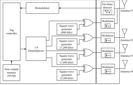
그림 1. 제안 태그의 블록도
Fig. 1. Block diagram of proposed tag system
표 1. 제안 구조에서 널 부반송파에 따른 허용되는 부
반송파 주파수
Table1. Allowed subcarriers for the proposed method.
Frequencies of null subcarriers (*1/Ts)
Allowed frequencies of subcarriers (*1/Ts)
0 1, 2, 4, 8, 11, 13, 16 1 2, 3, 4, 5, 7, 8, 11, 13, 16 1,2 3, 4, 5, 6, 7, 8, 10, 11, 13, 14, 16 1,2,3 4, 5, 6, 7, 8, 9, 10, 11, 13, 14, 15, 16
odd harmonic of the fundamental frequency. Hence, he frequency of the subcarriers must be assigned to avoid an overlapping with the harmonics of other subcarrier signals while maintaining the orthogonality of the subcarriers. For example, if a subcarrier with a frequency of 1/Ts is used, subcarriers with frequencies of 3/Ts, 5/Ts, …, (2k+1)/Ts must not be used. Table 1 shows the allowed subcarriers for some cases of the null subcarriers.* For example, as shown in 1st row in Table 1, if the DC is not used, the frequency of 1/Ts can be used as a subcarrier.
Since the square wave with a frequency of 1/Ts has every odd harmonic of 1/Ts, square waves with
* In Table 1, allowed subcarriers up to a frequency of 16/Ts
are shown as an example.
frequencies of 3/Ts, 5/Ts, …, (2k+1)/Ts must not be used. And, the frequency of 2/Ts can be used as a subcarrier because it is not a odd harmonic of 1/Ts.
표 2. 태그 송신, 리더 수신 개발 시스템 규격
Table2. Specifications of the tag-to-reader demonstration system.
Parameter Specification
Frequency band 917-923.5 MHz
Data rate 1.6 Mbps
Number of subcarriers 4
Subcarrier frequency spacing
Integer multiples of 400 kHz
Modulation ASK
Since the square wave with a frequency of 2/Ts has every odd harmonic of 2/Ts, square waves with frequencies of 3*2/Ts, 5*2/Ts, …, (2k+1)*2/Ts must not be used. And, the frequency of 4/Ts can be used as a subcarrier because it is not a odd harmonic of 1/Ts, nor that of 2/Ts.
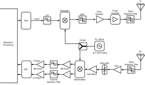
그림 2. 리더 RF 송수신기의 블록도
Fig. 2. Block diagram of reader RF transceiver.
Ⅲ. System Architecture and Function Blocks
Fig. 1 and Table 2 show a block diagram and the specifications of the proposed tag system, respectively.
The proposed system uses backscattering technique for tag-to-reader communication. Tag transmitter consists of four subcarrier modulators, four load modulators, and four antennas. As shown in Fig. 1, each load modulator uses its own load antenna. The load modulator is implemented using an Agilent HSMP 3822 PIN diode. In the demonstration system, the transmission bit rate of each subcarrier modulator is equal to 400 kbps. Frequencies of the subcarriers are 800 kHz, 1,200 kHz, 1,600 kHz, and 3,200 kHz, respectively.** The tag receiver consists of envelope detector and digital demodulator and is the same as existing UHF RFID tag receiver.
Fig. 2 shows a block diagram of the reader. Reader transmitter consists of digital modulator, DAC and direct RF up-converter. The resolution and sampling rate of the DAC are 12 bits and 5.12 MS/s, respectively. A modulator upconverts the baseband signals to 900 MHz RF band. Dielectric resonator type band-pass filter (BPF) is used to remove the
** The subcarrier frequencies are decided according to 2nd row in Table 1.
harmonics of the mixer output. The insertion loss of the BPF is less than 3 dB. Driver amplifier (DA) and power amplifier are used to transmit a continuous wave (CW) power level of 1W (30dBm). Lowpass type band selection filter is used to reject out-of-band interferers. The insertion loss of the band selection filter is about 0.5 dB in frequency band of 902 MHz to 928 MHz. The maximum output power of the power amplifier is 2 W (33 dBm).***
The RF receiver uses a direct-conversion receiver architecture. The band selection filter removes signals outside the 917 MHz to 923.5 MHz band. To prevent the saturation, the gain of LNA is set to 16 dB and the input P1dB of mixer is set to 13.2 dBm.
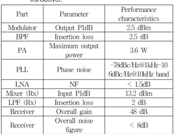
Attenuator is used to maximize the analog-to-digital converter (ADC) dynamic range while avoiding clipping. The mixer output is amplified by a linearized one-stage differential amplifier to provide gain before the channel selection filter. In addition, the channel selection filter output is amplified to use the full dynamic range of the ADC. The resolution and sampling rate of the ADC are 8 bits and 40.96 MS/s, respectively. Table 3 summarizes the performance characteristics of the reader RF transceiver.
*** According to local regulation in Korea, 4 W effective isotropic radiated power (EIRP) is allowed.
SFD detection
Carrier phase estimation
Carrier phase
compensation FFT decision
Signal detection
AGC
그림 3. 리더 디지털 복조기 블록도
Fig. 3. Block diagram of the digital demodulator in reader.
표 3. 리더 RF 송수신기의 성능 측정 결과
Table3. Performance characteristics of the reader RF transceiver.
Part Parameter Performance
characteristics
Modulator Output P1dB 2.5 dBm
BPF Insertion loss 2.5 dB
PA Maximum output
power 3.6 W
PLL Phase noise -78dBc/Hz@1kHz-10 6dBc/Hz@10kHz band
LNA NF < 1.5dB
Mixer (Rx) Input P1dB 13.2 dBm LPF (Rx) Insertion loss 2 dB
Receiver Overall gain 48 dB
Receiver Overall noise
figure < 8dB
Fig. 3 presents a block diagram of the digital demodulator in the reader. Based on the fact that the subcarriers in the tag are orthogonal, the digital demodulator is designed utilizing the OFDM demodulator architecture. Since the tag backscatters the reader's CW carrier, the carrier frequency of a tag is the same as that of a reader. Hence, carrier frequency offset compensation is not necessary in the reader demodulator, as shown in Fig. 3. The proposed tag transmit preamble signals for demodulation in the reader. The preamble uses the subcarrier with frequency of 2/Ts because signal with one frequency simplifies the digital demodulator in reader. The preamble consists of three signal sections. The first of these sections consists of four bits {1,0,0,1} and is used for signal detection. The number of bits of the first of preamble is decided by environmental conditions in which subcarrier frequency offset can be tolerated up to 0.1/Ts and system achieves a bit error rate (BER) of 10-5 at an Eb/N0 of 10.5 dB.
(a)
(b) 그림 4. 개발시스템 (a) 태그, (b) 리더
Fig. 4. Photographs of developed system (a) tag and (b) reader.
The second consists of 25 consecutive 0’s is used for a digital automatic gain control (AGC). In addition, the third consists of four bits and is used for start frame delimiter (SFD) detection. The signal detection is achieved using the cross-correlation between the first section of reference preamble and the received signal. The power of the second section of preamble is used for a digital AGC. The SFD detection is accomplished using the cross-correlation between the third section of reference preamble and the received signal. Since the demodulator utilizes an OFDM architecture, FFT is used for the demodulation.
Ⅳ. Experiment Results
Fig. 4 shows photographs of the developed system.
In Fig. 4(a), four SMA connector and four load modulators are shown. In Fig. 4(b), digital MODEM
(a) (b)
(c) (d)
(e)
그림 5. 태그의 부하변조 신호 (a)부반송파 : 800kHz, (b)부반송파 : 1,200kHz, (c)부반송파 : 1,600kHz, (d)부반송파 : 3,200kHz 와 (e) 4 부반송파를 모두 사용
Fig. 5. Load-modulated signals from the tag with subcarrier of (a) 800 kHz, (b) 1,200 kHz, (c) 1,600 kHz, (d) 3,200 kHz, and (e) all four frequencies.
This work Helleputte[17] Thomas[14]
Year 2010 2012
Communication technique
UHF RFID
(ASK-OFDM) IR-UWB UHF RFID (QPSK) Power
consumption
9 uW
(analog part) 3.3mW 0.12 uW (analog part) Frequency 902-928 MHz 0-960 MHz 850-950 MHz Data rate 1.6 Mbps 19.5 Mbps 0.4 Mbps Req. Eb/No
(BER=10-4) 9.2 dB - 11.5 dB
Battery use
(analog part) No Yes Yes
표 4. 대표적인 초저전력 통신 기술 비교
Table4. Comparison with representative ultra low-power communication techniques.
그림 6. 4 부반송파 기반의 부하변조 스펙트럼
Fig. 6. PSD of load-modulated signals with four subcarriers.
and RF transceiver are implemented in left part and right part, respectively. For measurement, the reader uses a separate transmit and receive antenna to reduce leakage from the transmitter to the receiver.[1
6]**** Fig. 5 shows the load-modulated signals from the tag.***** In Fig. 5(a)-(d), each data is modulated with subcarriers of 800 kHz, 1,200 kHz, 1,600 kHz, and 3,200 kHz, respectively. In Fig. 5(e), four subcarriers are used to modulate four bits. Fig. 6 shows a measured power spectral density (PSD) of load-modulated signals from the tag with four subcarriers of Fig. 5(e). Fig. 7 shows the measured
**** This antenna arrangement is known as a bistatic configuration.
***** In Fig. 5, green and dark green lines are I channel and Q channel demodulated signals, respectively.
1E-05 1E-04 1E-03 1E-02
5 6 7 8 9 10
Eb/N0(dB)
measurement theory
Bit Err or R ate (BE R)
그림 7. 비트오율 측정 결과
Fig. 7. Measured BER performance.
BER performance.* The system produces a BER of 10-5 at an Eb/N0 of 10.8 dB. This degradation is caused by implementation loss in subcarrier frequency offset compensation and phase recovery. In Table 4, proposed tag system is compared with representative ultra low-power communication techniques. As aforementioned in Section I, QPSK based UHF RFID tag has a SNR degradation of about 2.3 dB.
V. Conclusion
This paper presented a square-wave subcarrier-based OFDM technology for a tag-to-reader communication link. The tag used multiple load modulators to remove DACs. Each load modulator was modulated with a different square-wave subcarrier signal. The hardware measurement results showed a BER of 10-5 at an Eb/N0
of 10.8 dB.
REFERENCES
[1] K. Finkenzeller, RFID Handbook, 2nd ed., West Sussex, England, Wiley, 2003.
[2] ISO/IEC 18000-6, Information technology-Radio Frequency Identification for Item Management -
*To measure the BER performance, the transmitter, receiver, and AWGN signal generator are connected using a cable, and an adjustable attenuator is used to sweep the receiver input power.
Part 6: Parameters for Air Interface Communication at 860 MHz to 960 MHz, 2nd ed., International Organization for Standardization, Dec. 2010.
[3] S. Choi et al., “A Fully Integrated CMOS Security-Enhanced Passive RFID Tag,” ETRI J., vol. 36, no. 1, pp. 141-150, Feb. 2014.
[4] Evizal, T. A. Rahman, and S. K. Rahim, “RFID Vehicle Plate Number (e-Plate) for Tracking and Management System,” Proc. Int. Conf. Parallel and Distributed Systems, pp. 611-616, Seoul, Korea, Dec. 15-18, 2013.
[5] C. R. Medeiros et al., “UHF RFID Cabinet,”
Proc. Int. Symp. Antennas and Propagation, pp.
1429-1432, Spokane, U.S.A, Jul. 3-8, 2011.
[6] A. C. Polycarpou et al., “A Healthcare Application based on Passive UHF RFID Technology,” Proc. European Conf. Antennas and Propagation, pp. 2814-2818, Rome, Italy, Apr.
11-15, 2011.
[7] X. Li et al., “Customer Service Enhancement using Passive RFID,” Proc. IEEE Int. Conf.
Comm. Technol. and Applications, pp. 5-9, Beijing, China, Oct. 16-18, 2009.
[8] J.-H. Bae et al., “Design of Reader Baseband Receiver Structure for Demodulating Backscattered Tag Signal in a Passive RFID Environment,”
ETRI J., vol. 34, no. 2, pp. 147-158, Apr. 2012.
[9] I. Choi, M. Cha, and I. Kwon, “A Integrated TX Leakage Canceller for UHF RFID Reader,” Proc.
IEEK Summer Conf., pp. 426-429, Jun. 2011.
[10] S. Nam, J. Ahn, and D. Kim, “Evaluation of RFID System for Location Based Services in the Building,” J. of Institute of Electronics Engineers of Korea, vol. 48, no. 1, pp. 45-50, Mar. 2011 [11] D. Dardari et al., “Ultrawide Bandwidth RFID: The
Next Generation?,” Proc. IEEE, vol. 98, no. 9, pp.
1570-1582, Sep. 2010.
[12] N. Kim et al., RFID System, US Patent 2008/0290997. 2008.
[13] S. J. Thomas, J. S. Besnoff, and M. S. Reynolds,
“Modulated Backscatter for Ultra-Low Power Uplinks from Wearable and Implantable Devices,”
Proc. ACM workshop Med. Commun. Sys., pp.
1-6, Helsinki, Finland, Aug. 13-17, 2012.
[14] S. J. Thomas, E. Wheeler, J. Teizer, and M. S.
Reynolds, “Quadrature Amplitude Modulated Backscatter in Passive and Semi-Passive UHF RFID Systems,” IEEE Trans. Microwave Theory Tech., vol. 60, no. 4, pp. 1175-1182, Apr. 2012.
[15] R. van Nee and R. Prasad, OFDM for Wireless Multimedia Communications. Boston, MA: Artech House, 2000.
[16] D. M. Dobkin, The RF in RFID: Passive UHF RFID in Practice, Elsevier, pp. 171-179, 2008.
[17] N. Helleputte et al., “A Reconfigurable, 130nm CMOS 108 pJ/pulse, Fully Integrated IR-UWB Receiver for Communication and Precise Ranging,”
IEEE J. Solid-State Cir., vol. 45, no. 1, pp. 69-83, Jan. 2010.
저 자 소 개 박 형 철(정회원)
1996년 한국과학기술원 전기 및 전자공학과 학사 1998년 한국과학기술원 전기 및
전자공학과 석사
2003년 한국과학기술원 전자 전 산학과 박사
2003년∼2005년 하이닉스반도체 선임연구원 2005년∼2010년 한밭대학교 정보통신컴퓨터공
학부 전임강사/조교수
2010년∼현재 서울과학기술대학교 전자IT미디어 공학과 조교수/부교수
<주관심분야 : 변복조 알고리즘, 통신VLSI>