고전압 동작용 I/O 응용을 위해 Counter Pocket Source 구조를 갖도록 변형된 DDD_NSCR 소자의 ESD 보호성능 시뮬레이션
서용진*, 양준원** 정회원
Simulation-based ESD protection performance of modified DDD_NSCR device with counter pocket source structure for high
voltage operating I/O application
Yong-Jin Seo*, Jun-Won Yang** Regular Members
요 약
종래의 이중 확산된 드레인을 갖는 n형 MOSFET(DDD_NMOS) 소자는 매우 낮은 스냅백 홀딩 전압을 갖는 SCR 특성을 나타내므 로 정상적인 동작 동안 래치업 문제를 초래한다. 그러나, 본 연구에서 제안하는 counter pocket source (CPS) 구조를 갖도록 변형된 DDD_NMOS 구조의 SCR 소자는 종래의DDD_NSCR_Std 표준소자에 비해 스냅백 홀딩 전압과 온-저항을 증가시켜 우수한 정전기 보호 성능과 높은 래치업 면역 특성을 얻을 수 있는 것으로 확인되었다.
Key Words : ESD, DDD_NMOS, DDD_NSCR_CPS, CPS, snapback holding voltage, on-resistance, latch-up immunity, simulation
ABSTRACT
A conventional double diffused drain n-type MOSFET (DDD_NMOS) device shows SCR behaviors with very low snapback holding voltage and latch-up problem during normal operation. However, a modified DDD_NMOS-based silicon controlled rectifier (DDD_NSCR_CPS) device with a counter pocket source (CPS) structure is proven to increase the snapback holding voltage and on-resistance compare to standard DDD_NSCR device, realizing an excellent electrostatic discharge protection performance and the stable latch-up immunity.
*세한대학교 소방행정학과/나노정보소재연구소 ([email protected])
**세한대학교 항공교통물류학과 ([email protected]), 교신저자 : 양준원
※ 본 연구는 2016년도 세한대학교 교내 연구비 지원에 의하여 수행되었음.
접수일자 : 2016년 11월 22일, 수정완료일자 : 2016년 12월 5일, 최종게재확정일자 : 2016년 12월 6일
I. Introduction
Electrostatic discharge (ESD) protection is a critical issue in high-voltage operating microchips. Traditionally, n-type metal-oxide semiconductor field-effect transistor (NMOSFET) devices have been adopted as ESD protection devices for input/output (I/O) cell applications.
However, it is difficult to achieve the ESD protection in the high voltage operating double diffused drain n-type MOSFET (DDD_NMOS) devices due to the non-uniform current flow[1]. Remarkably strong snapback characteristics induce current crowding effect and
consequential melting damages[1-3]. Studies for realizing a stable ESD protection performance in these devices made some meaningful progresses; however, their practical usages are somehow limited because of a decreased operation voltage[3-4]. Since the self-protection strategy using a DDD_NMOS device is practically impossible in the high voltage operation range, alternative approaches have to be searched. Among various ESD protection devices, a high-voltage operating DDD_NMOS-based silicon controlled rectifier (DDD_NSCR) device is an attractive candidate owing to its high current immunity level[5-8]. However, the high
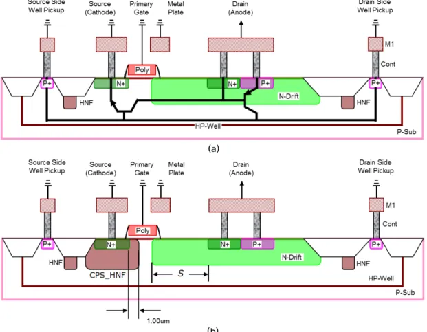
(a)
(b)
Fig. 1. (a) Schematic diagram of high-voltage operating standard DDD_NSCR_Std device. In this device, the N- drift edge to N+ diffusion space (S) is set to be 1.6 µm. (b) Schematic diagram of modified DDD_NSCR_CPS with a CPS structure. In the DDD_NSCR_CPS device, the N- drift edge to N+ diffusion space (S) is change from 0.8 µm to 1.6 µm. (where, M1: Metal 1, Cont: via Contact, Poly: Poly-silicon gate, HP-Well; High P-type Well, P-Sub: P-type Substrate, CPS: Counter Pocket Source, HNF: High N-stop Field implantation, respectively) voltage operating SCR (HV_SCR) device is very
vulnerable to a latch-up problem during a normal operation. Extensive studies have been devoted to solve this problem; however, such works have ended with only limited successes[9-12]. The high vulnerability of the HV_SCR device to the latch-up problem results from an extremely low on-resistance and a consequential low snapback holding voltage in high current limit. Thus, a junction/channel engineering technique for increasing the on-resistance in the high current limit may be effective for curing the problematic points of this device.
In this work, a modified DDD_NSCR_CPS device with a p-type counter pocket source (CPS) structure enclosing N+source region is proposed in order to achieve the ESD protection for high voltage operating I/O application.
Methodology for the modification engineering and the related operation mechanisms are discussed in terms of thermal effects incorporated two-dimensional (2D) device simulation results. The proposed DDD_NSCR_CPS device reveals the excellent ESD protection performance and the high latch-up immunity. Since the CPS implant technique
does not change avalanche breakdown voltage, this methodology does not reduce available operation voltage and is applicable regardless of the operation voltage.
Ⅱ. Device structure and analysis methodology
The DDD_NSCR device is constructed based on the DDD_NMOS structure with extended drain structure (i.e.
non-adjacency of the N+drain diffusion from the gate);
the P+diffusion is inserted into the N-drift region on the drain side to form a part of anode electrode as shown in Fig. 1(a). The resulting structure becomes a HV_SCR device consisting of a lateral NPN bipolar junction transistor (BJT) and vertical PNP-BJT. For the ESD application, the anode is connected to each I/O pad (or to Vdd power pad), while the cathode is connected to Vss
ground pad. The conventional DDD_NSCR_Std device is based on normal DDD_NMOS device without modification on the junction/channel region. In the modified
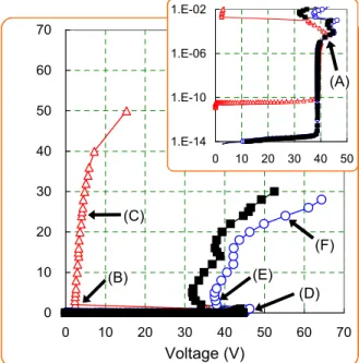
0 10 20 30 40 50 60 70
0 10 20 30 40 50 60 70
Voltage (V)
Anode Current (mA/um)
1.E-14 1.E-10 1.E-06 1.E-02
0 10 20 30 40 50 (A)
(B) (C)
(E)
(F)
(D) 0
10 20 30 40 50 60 70
0 10 20 30 40 50 60 70
Voltage (V)
Anode Current (mA/um)
1.E-14 1.E-10 1.E-06 1.E-02
0 10 20 30 40 50 (A)
(B) (C)
(E)
(F)
(D)
Fig. 2. Simulation results on I-V relations for DDD_NSCR devices (open triangle △ for DDD_NSCR_Std with S = 1.6 µm, open circle ○ for DDD_NSCR_CPS with S = 1.6 µm, closed square ■ for DDD_NSCR_CPS with S = 1.0 µm). Graphs in the inset represent same I-V relations with y-axis on log scale. (where, (A) & (D) = triggering point, (B) & (E) = snapback holding point, and (C) & (F)
= thermal breakdown point, respectively).
DDD_NSCR_CPS device, the p-type counter pocket source (CPS) implant [boron, 180 keV, 8.5x1013 cm-3, this structure corresponds to CPS_HNF of Fig. 1(b)] is added to enclose the N+cathode (source) diffusion region. The CPS implant dose and energy can be varied centering on the N- drift implant condition. As a result, the junction/channel profile is modified. Moreover, effective p-type doping outside the N+cathode diffusion region is drastically changed. The overlap margin of N+ anode (drain) diffusion over N-drift region [parameter ‘S’ in Fig.
1(b)] is either kept same with that of DDD_NSCR_Std, or made smaller. The overlap margin is varied from 0.8 to 1.6 µm.
The characteristics of the DDD_NSCR devices are investigated by a 2D process and device simulation. The devices are fabricated using a TSUPREM4 (Synopsis Co.) process simulator following a high-voltage operating (Vop
≈ 30 V) technology. The device characteristics are analyzed using a DESSIS (ISE Co.) device simulator. In a low current limit with a device current lower than 1x10⁻⁵ A/µm, a non-thermal DC simulation is performed. In a high current limit with a device current higher than 1x10⁻⁵ A/µm, a thermally incorporated mixed mode transient (MMT) simulation is performed, incorporating thermal effects. In this transient simulation, ladder-type current pulses with a rise time of 10 ns and a duration of 100 ns are applied to simulate a human body model (HBM) ESD stress.
Ⅲ. Results and discussion
Simulation deduced I-V relations of the DDD_NSCR_Std device clearly shows typical SCR-like characteristics as shown in (A), (B), and (C) of Fig. 2.
They are also characterized by a high current immunity level (about ≈ 50 mA/µm), an extremely low snapback holding voltage (Vh ≈ 2.3 V), and a low on-resistance (Ron≈ 271 Ω∙µm). The snapback holding voltage (Vh) is much smaller than the operating voltage (Vop ≈ 30 V).
This implies that the DDD_NSCR_Std device, when used as a power clamp ESD protection device between Vddand Vss pad, becomes very vulnerable to latch-up problem during normal operation.
Being different from those of the DDD_NSCR_Std device, theI-V curves of the DDD_NSCR_CPS device as shown in (D), (E), and (F) of Fig. 2 are characterized by a relatively high snapback holding voltage (Vh≈ 43.3 V) and a high on-resistance (Ron ≈ 1121 Ω∙µm). The
snapback holding voltage (Vh ≈ 43.3 V) is shown to be higher than the operating voltage (Vop ≈ 30 V). Thus, latch-up immunity is guaranteed. The relatively high snapback holding voltage and high on-resistance result in a thermal breakdown voltage (Vtb ≈ 64.4 V) larger than the triggering voltages (Vtr1≈ 45 V and Vtr2 ≈ 46 V), which guarantees a uniform multi-finger triggering and a stable current immunity level linearly against the finger number. It should be emphasized that the CPS implant engineering decreases neither the avalanche breakdown voltage (Vav≈ 38.7 V) nor the triggering voltages (Vtr1≈ 45 V and Vtr2 ≈ 46 V) when compared with the DDD_NSCR_Std device. This implies that the methodology of this CPS implant technique, since it does not reduce the available operation voltage, is applicable to any operation voltage. The off-state leakage current of the DDD_NSCR_CPS device decreases by almost 4 orders due to the CPS implant. Current immunity level of the DDD_NSCR_CPS device decrease down upon modification.
However it is still high enough for area-efficient ESD protection performance. Current capacity of the DDD_NSCR_CPS device is estimated to ≈ 3 A for device width of 100 µm.
Also,I-V characteristics are strongly dependent on the
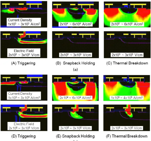
(a)
(b)
Fig. 3. Contour data of current density and electric field at the triggering point (A, D), at the snapback holding point (B, E) and at the high current region near thermal breakdown point (C, F) of Fig. 2. Contours at (A), (B) and (C) represent for the DDD_NSCR_Std (S = 1.6 um) device and those at (D, E, F) represents for DDD_NSCR_CPS (S = 1.6 um) device. The numbers within each picture represent the range of the corresponding the current density value or electric field value. (a) DDD_NSCR_Std device, (b) DDD_NSCR_CPS device.
overlap margin of anode N+ diffusion over the N- drift region [parameter S of Fig. 1(b)]. Reduction of the parameter S results in the shrinkage of the effective base width between the two electrodes. This shrinkage causes in a little smaller triggering voltage and lower Vh, which guarantees more flexibility in the optimization for ideal ESD protection performance. It should be noted that too much reduction in parameter S results in decreases in avalanche breakdown voltage and its corresponding available operation voltage. Thus, the parameter S should be reduced only within a certain limited range so as not to change the avalanche breakdown voltage.
Corresponding contour data provide phenomenological explanation on the drastic change of theI-V relations as shown in Fig. 3. At the BJT triggering point [(A) and (D) of Fig. 3], the depletion induced high electric field region is formed along the N-drift/HP-well border. It seems that only the lateral NPN-BJT operation is initiated at the very beginning of the triggering point, which is justified by the overwhelming surface current path between drain N+and source N+diffusions. This is qualitatively same regardless
of the device type [refer (A) and (D) points of Fig.3].
However, when the DDD_NSCR_Std enters the snapback holding point or higher current region [refer (B) and (C) points of Fig. 3, respectively], the vertical PNP-BJT operation is also initiated and combines with the lateral NPN-BJT operation to induce the resultant PNPN-SCR operation. Thus, the current path becomes a widely distributed U-shaped path. The high electron injection from the cathode N+diffusion leads to the deep electron channeling under the gate. That is, the background doping of the HP-well and the N- drift region is completely screened by the injected free carriers. Thus, the whole current path between the cathode and the anode becomes field-free, as explicitly shown in the corresponding electric field contour of Fig. 3. The low Vh and low Ron can be explained in terms of the field-free and wide current path between two electrodes. High electron injection induced base push out (or Kirk effects) and the consequential low Vh and the low Ron had been addressed in the precedent works[3][11].
Talking on the contour data of the DDD_NSCR_CPS
device as shown in (E) and (F) of Fig.3, due to CPS implant, the lateral directional high electric field region still survives even at the snapback holding or at higher current level. That is, the lateral directional high-density electron surge from source N+diffusion is blocked owing to the CPS implant, such that the base-push out does not occur. The widely distributed U-shaped current path evokes upon the PNP-BJT operation and the subsequent PNPN-SCR operation is initiated. However, since the high electric field region remains in the direction of the current path, the snapback holding voltage does not markedly decrease. When the anode current increases further after the snapback holding state, the high electric field region along the bottom directional N-drift/HP-well border line seems to be smeared out gradually. However, the high electric field region along the lateral directional N- drift/HP-well border line is never smeared out. Moreover, the newly arising high electric field region is formed in the direction of the U-shaped main current path. These may explain the relatively high on-resistance(Ron) and marked increase in the local maximum temperature in the high current region near the thermal breakdown point (F).
Ⅳ. Conclusion
The simulation analysis results suggest that our modified DDD_NSCR_CPS device demonstrates both the robust ESD protection characteristics and high latch-up immunity. The CPS implant and the overlap margin of the anode N+diffusion over the N-drift are critical factors in the amendment engineering. The CPS implant is never affects the avalanche breakdown voltage of the device.
Thus, this methodology does not change the available operation voltage and is applicable regardless of the operation voltage. In conclusion, the DDD_NSCR_CPS device can be a promising ESD protection device for high voltage I/O applications.
References
[1] Mergens M, Wilkening W, Mettler S, Wolf H, Stricker A, Fichtner W, “Analysis of lateral DMOS power devices under ESD stress conditions”, IEEE Trans Electron Devices, 47(11), pp.2128–2137, 2000.
[2] Dabral S, Maloney T, “Basic ESD and I/O Design”, John Wiley & Sons, 1998.
[3] Jeon B-C, Lee S-C, Oh J-K, Kim S-S, Han M-K, Jung Y-I, Kim K-H, “ESD characterization of grounded-gate NMOS with 0.35 lm/18 V technology employing transmission line pulser (TLP) test”, In Proceedings of the EOS/ESD symposium, pp.362–372, 2002.
[4] Kim K-H, Jung, Y-I, Shim, J-S, So H-T, Lee J-H, Hwang L-Y, Park J-W, “Illumination of double snapback mechanism in high voltage operating grounded gate extended drain N-type metal-oxide-semiconductor field effects transistor electro-static discharge protection devices”, Japanese journal of applied physics, 43(10), pp.6930-6936, 2004.
[5] Chatterjee A, Polgreen T, “A low-voltage triggering SCR for on-chip ESD protection at output and input pads”, IEEE Electron Device Lett., 12(1), pp.21–22, 1991.
[6] Lee J-H, Shih J-R, Tang C-S, Liu K-C, Wu Y-H, Shiue R-Y, T-C. Ong, Y'-K Peng, J-T Yue,“Novel ESD protection structure with embedded SCR LDMOS for smart power technology”, In Proceedings of the IEEE 40th annual international reliability physics symposium, pp.156–161, 2002.
[7] Ker M-D, Chang H-H, Wu C-Y, “A gate-coupled PTLSCR/NTLSCR ESD protection circuit for deep-submicron low-voltage CMOS IC’s”, IEEE J Solid-State Circuits, 32(1), pp.38–51, 1997.
[8] Lai C-H, Liu M-H, Su S, Lu T-C, Pan S, “A novel gate-coupled SCR ESD protection structure with high latchup immunity for high-speed I/O pad”, IEEE Electron Device Lett., 25(5), pp.328–330, 2004.
[9] Ker MD, “Lateral SCR devices with low-voltage high-current triggering characteristics for output ESD protection in submicron CMOS technology”, IEEE Trans Electron Dev., 45(4), pp.849–860, 1998.
[10] Mergens M, Russ C, Verhaege K, Armer J, Jozwiak P, Mohn R, “High holding current SCRs (HHI-SCR) for ESD protection and latch-up immune IC operation”, In Proceedings of the EOS/ESD symposium, pp.14–21, 2002.
[11] Streibl M, Esmark K, Sieck A, Stadler W, Wendel M, Szatkowski J, Gobner H, “Harnessing the base-pushout effect for ESD protection in bipolar and BiCMOS technologies”, In Proceedings of the EOS/ESD symposium, pp.73–82, 2002.
[12] Kim K-H, Seo Y-J, “Electronic discharge (ESD) protection of N-type silicon controlled rectifier with P-type MOSFET pass structure for high voltage operating I/O application”, Microelectronics Reliability, 53(2), pp.205-207, 2013.
저자
서 용 진(Yong-Jin Seo) 정회원
․1987년 2월:중앙대학교 전기공학과 학사졸업
․1989년 2월:중앙대학교 전기공학과 석사졸업
․1994년 2월 : 중앙대학교 전기공학과 박사졸업
․1995년 3월 ∼ 현재:세한대학교 교수
․2004년 3월 ∼ 현재 : 세한대학교 나노정보소재연구소 소장
<관심분야> : 반도체소자, 정전기보호소자, CMP공정
양 준 원(Jun-Won Yang) 정회원
․1989년 2월:영남대학교 전자공학과 학사졸업
․1995년 3월:Keio대학교 이공학연구과 전기공학과 석사졸업
․1999년 3월:Keio대학교 이공학연구과 전기공학과 박사수료
․1999년 3월 ∼ 현재:세한대학교 교수
<관심분야> : 위성통신, 전자파 해석