- 1353 -
유기박막 트랜지스터로의 응용을 위한 플라즈마 중합 고분자 박막
임재성1,2, 신백균2, 이붕주3, 유도현4, 박세근1, 이일항1
인하대학교 집적형광자기술연구센터1, 인하대학교 전기공학과2, 남서울대학교 전자공학과3, 안산공과대학 전기과4
The plasma polymerized polymer thin films for application to organic thin film transistor
Jae-Sung Lim1,2, Paik-Kyun Shin2, Boong-Joo Lee3, Do-Hyun You4, Se-Geun Park1, El-Hang Lee1 Optics and Photonics Elite Research Academy1, Inha Univ.2, Namseoul Univ.3, Ansan Tech. Coll.4
Abstract - The OTFT devices had inverted staggered structures of Au/pentacene/ppMMA/ITO on PET substrate. The overall device performances of the flexible devices such as the operating voltage, the field effect mobility, the on/off ratio and the off current are somewhat worse than those of devices fabricated on glass substrates. Pentacene/ppMMA OTFT benchmarks (mobility, sub-threshold slope, on/off ratio) were comparable to that of solution cast PMMA, but below average when compared to other polymer gate dielectrics. However, threshold and drive voltages were among the lowest reported for a polymer gate dielectric, and surpassed only by ultra-thin SAM gate dielectrics.
1. Introduction
The availability of organic semiconductor devices may open the way to completely new set-ups, fabrication processes, and applications. The problem of operating voltage for flexible OTFT could thus potentially be solved by using thin gate dielectric layer of polymer materials [1]. Dielectric materials of polymer may be deposited by solution processes such as conventional spin-coating, dip-coating, and inkjet printing. These techniques provide a potential niche for polymers in applications that require large areas process, low cost, mechanical flexibility, and a combination of these factors.
In order to realize a flexible flat panel display based on promising performance of OLEDs, pixel control semiconductor device, namely thin film transistor (TFT), should also be fabricated using organic materials and appropriate process technologies compatible with organic materials. An organic thin film transistor (OTFT) might be a promising candidate for this kind of application. Main criterion in OTFT is relatively high operation voltage which is mainly caused by inferior permittivity/capacitance property through relatively thick gate dielectrics. A thin polymer dielectric having high permittivity could be a solution to overcome this problem. Polymer dielectrics can be deposited by solution processes such as spin-coating, dip coating, and inkjet printing. But these wet-processes would cause possibly overall degradation of the device performance. A dry fabrication process for polymer dielectric might be a solution to avoid such problems. In addition, plasma polymerization technique would be an alternative to prepare the polymer gate dielectric. Plasma polymerized polymers show different characteristics from those of conventionally prepared polymers in two ways:
(1) the materials show highly cross-linked structure; (2) chemical structure of the monomer is not necessarily preserved through the process of fragmentation and recombination within the plasma environment. Because of their unique properties, plasma polymerized films have been used in a variety of applications including barrier coatings, protective coatings, selective permeation membranes. Moreover, plasma polymerized polymers have interesting properties and it can be successfully utilized as electron-beam resists.
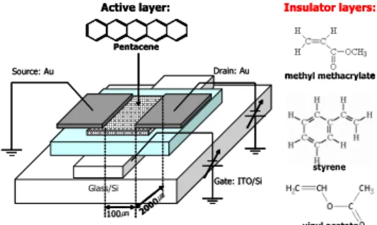
In this thesis, plasma polymerized methyl methacrylate (ppMMA), styrene (ppS), and vinyl acetate (ppVA) polymer thin films were deposited using a r.f. 13.56 plasma polymerization process. The plasma polymerized polymer thin films were then applied to an OTFT device fabrication which was carried out by an exclusively dry process. The OTFT device was fabricated either on a ITO/glass substrate and or on ITO/PET flexible substrate, where thermally evaporated pentacene and Au were active channel layer and source/drain electrode, respectively.
2. Experimental 2.1 Plasma treatment & plasma polymerization
ITO-coated glasses (Samsung Corning co.) were used as substrates, where ITO was 150-nm-thick and had sheet resistance of 12 Ω/□. The substrates
were ultrasonically cleaned in acetone, ethanol and DI-water, by which most of the ITO surface organic contaminants were removed. The surface of ITO gate electrode was then treated in an Ar plasma prior to depositions of insulating layer. A r.f. capacitively-coupled plasma (CCP) was used for surface treatment of the ITO gate electrode: pressure of 0.1 Torr, Ar flow rate of 10 sccm, and r.f. main power of 100 W, respectively. It is shown that surface roughness of the ITO tends to decrease after the Ar plasma treatment with a limited treatment time. In addition, due to the ppMMA layer giving a conformal coverage of the ITO spikes and pinhole, ITO surface has a smooth morphology interface with good contact for the pentacene deposition, resulting the field effect mobility is increased. Without breaking vacuum after the plasma surface treatment, plasma polymerized methyl methacrylate, styrene, and vinyl acetate insulting layer was then prepared, where a monomer (Sigma-Aldrich co.) was used, respectively.
Plasma polymerization of the polymer dielectric layers was done again using a r.f. capacitive-coupled plasma (CCP) equipment. Figure 3.6 shows a schematic of the equipment, by which both the ITO surface treatment and plasma polymerization were carried out. The ppMMA was deposited under following experimental condition; main power of 200 W/bias power of 20 W, system pressure of 0.5 Torr, Ar flow rate of 20 sccm, and deposition time of 1~20 min, respectively. Figure 3.7 shows schematic of OTFT and chemical structures of materials used in this thesis.
2.2 Thermal evaporation
Pentacene and Au films were deposited with constant deposition rate of 0.5 and 1.0 Å/s at substrate temperature of room temperature, respectively.
A 60-nm-thick pentacene (Sigma-Aldrich co.) as active channel layer, and 100-nm-thick Au as source/drain electrode layer were then deposited using thermal evaporation technique: the Au source/drain electrodes was patterned on pentacene layer through a shadow mask. The OTFT devices had inverted staggered structures of Au/pentacene/plasma polymerized polymers/ITO.
Figure 1 shows a schematic diagram of the OTFTs fabricated in this thesis.
Drain: Au Source: Au
Gate: ITO/Si Glass/Si
100㎛ 2000㎛
methyl methacrylate
styrene
vinyl acetate Insulator layers:
Pentacene Active layer:
Drain: Au Source: Au
Gate: ITO/Si Glass/Si
100㎛ 2000㎛
methyl methacrylate methyl methacrylate
styrene styrene
vinyl acetate vinyl acetate Insulator layers:
Pentacene Active layer:
<Figure 1> Schematic of OTFT and chemical structures of materials used in this study.
2.3 Characterization of materials and OTFTs
Chemical composition, surface energy, and electrical properties of the plasma polymerized polymers were investigated using Fourier transform infrared spectroscopy (FT-IR; Vertex 80v, Bruker Optics) in vacuum, contact angle meter (Erma inc.), respectively. For investigating performance of the OTFTs, current-voltage (I-V) characteristics according to applied voltage change were measured by a source measurement unit (Keithley 236) combined with a source measurement unit (Keithley 2400): for the I-V measurement, time delay for each measurement was 0.5 sec, and sampling width was 0.1 V.
2009년도 대한전기학회 하계학술대회 논문집 2009. 7. 14 - 17
- 1354 -
3. 결과 및 고찰 3.1 Fourier transform-infrared spectroscopy
Figure 2 shows the FT-IR absorption spectra of plasma polymerized polymer dielectric layers. In order to characterize the polymers, ppMMA, ppS, and ppVA films were deposited on a KBr substrate, and their FT-IR spectroscopy were analyzed. In the ppMMA, these PMMA absorbance characteristic peaks are comparatively weak and broader (but not absent), suggesting significant amount of fragmentation and rearrangement in the plasma deposition process. One of the problems, hysteresis of OTFT devices is known to be caused by the impurities and trapped charges at the semiconductor/dielectric interface and those in the bulk of the dielectric and the inherent properties of the dielectric. To confirm this, the FT-IR absorption spectra was observed, as shown in Figure 2. The attribution of the bands can be given as follows: the bands at 3400 cm-1 are attributed to the O-H groups.
4000 3500 3000 2500 2000 1500 1000 500
OH CH C=CCH
C-O C=O
Absorbance (a.u.)
Wavenumber (cm-1)
4000 3500 3000 2500 2000 1500 1000 500
C-O CH
C=C C=O
CH OH
Absorbance (a.u.)
Wavenumber (cm-1)
<Figure 2> FT-IR spectra of (a) ppMMA, (b) ppVA, and (c) ppS.
3.2 Contact angle & Surface energy
Improved mobility could be depicted by changes in the surface energy of gate dielectrics [2]. In addition, lowering the surface energy on a gate dielectric was identified as a key factor to increase the grain size during the growth of pentacene. To evaluate those parameters related to the thin-film surface energy, we utilize Eq. 1, obtained from both Young’s equation and the equation of state for solid/liquid interfacial tension, to estimate the surface energy of gate dielectrics [2].
2 / 1 2 /
1 2( )
) ( 2 ) cos 1
( plp
p s d pl d s
pl γ γ γ γ
γ
θ = +
+ (1)
where and are the surface energies of the sample and the probe liquid, respectively, and the superscripts d and p refer to the dispersion and polar (nondispersion) components of the surface energy, respectively. This similar surface energy suggests that it may be possible to develop more efficient transistor channels by better matching the surface energies of the insulator and the pentacene. The surface energy of ppVA increased dramatically compared to that of ppMMA and ppS. Surface energy of the ppMMA dielectric was calculated from contact angle measurements using DI-water (about 61.5°) and methylene iodide (about 37°) as probe liquids.
The surface energy of the ppMMA dielectric was about 50 mJ/m2, which was similar to that of pentacene (49 mJ/m2), which suggests that it might be possible to develop more efficient OTFTs channel by matching the surface energy of the ppMMA dielectric and the pentacene [3].
3.3 Electrical properties
The characteristic electric properties of the devices are summarized in Table 1. Field-effect mobilities of 0.01-0.08 cm2V-1s-1 and threshold voltages of -3.0 to -3.3 V were obtained. This result agrees with previous results.
Surprisingly, the field-effect mobility increases by a factor of approximately 2 with only a small change 3.66-3.86, increase in the dielectric constant, , of the insulator.
The OTFT device with the ppMMA insulator was found to have a higher field effect mobility of 0.08 cm2V-1s-1 in the saturation region, a threshold voltage of -3 V, a low sub-threshold slope of 0.959 V/decade, and an on/off current ratio (Ion/Ioff) of 1×10⁴, respectively. It is highly likely that such favorable electrical properties of the OTFT device using relatively thin (100 nm) ppMMA with higher dielectric constant (=3.86) may be due to their enhanced polarization, which is possibly resulted in enhanced channel growth at the pentacene layer. This combination of favorable properties demonstrates that the OTFT can be operated successfully at voltages -10 V.
<Table 1> Properties of OTFTs with plasma polymerized polymer insulators.
Plasma polymeriz
ed polymersa
Insulator Device
Surface energy (mJ/m2)
Dielectri c constantb
Field-eff ect mobility (cm2V-1s-
1)
On/off current ratio
Threshol d voltagy
(V)
Sub-Thre shold slope (V/dec.)
Ioff
current (A)
ppMMA 50 3.86 0.08 1×10⁴ -3 0.959 1×10⁻¹⁰
ppS 47 3.66 0.05 5×10³ -3 0.634 4×10⁻¹⁰
ppVA 64 5.84 0.01 8×10² -3.3 0.470 4×10⁻¹⁰
a 100-nm-thick polymers.
b Measured at 100 kHz.
The OTFT devices had inverted staggered structures of Au/pentacene/ppMMA/ITO on PET substrate. The overall device performances of the flexible devices such as the operating voltage, the field effect mobility, the on/off ratio and the off current are somewhat worse than those of devices fabricated on glass substrates.
0 -2 -4 -6 -8 -10
0.0 -1.0x10⁻⁷ -2.0x10⁻⁷ -3.0x10⁻⁷ -4.0x10⁻⁷
VG = -0V, VG = -2V, VG = -4V VG = -6V VG = -8V VG = -10V
ID (A)
VD (V)
-10 -8 -6 -4 -2 0
0.0000 0.0001 0.0002 0.0003 0.0004 0.0005 0.0006 0.0007
µFET = 0.02 cm2V-1s-1 Slope = -8.398 X 10⁻⁵
Subthreshold slope
= 0.538 V/decade VD = -10V
VG (V) -ID1/2(A1/2)
10-10 10-9 10-8 10-7 10-6
-ID (A)
<Figure 3> Characteristics of flexible OTFTs.
4. Conclusion
An OTFT device with inverted staggered structure of Au/pentacene/ppMMA/ITO was fabricated. Proposed plasma polymerization method could be applied to a completely dry process for the OTFT fabrication, which offers an easy and low-cost alternative. It was demonstrated in this thesis that the ppMMA thin film can be used as insulators for organic semiconductors by preparing a high-performance device with -10 voltage operation. Test OLED/OTFT devices fabricated on a ITO/PET flexible substrate showed a possibility of further progress in flexible display with active matrix OLED configuration using OTFT as a pixel control semiconductor.
[Acknowledgement]
This work was supported by the Korea Science and Engineering Foundation through the Grant for the Integrated Photonics Technology Research Center (R11-2003-022) and by the Regional Innovation Center for Environmental Technology of Thermal Plasma (ETTP) at Inha University designated by MKE (2009)
[References]
[1] H. Klauk, “Organic electronics, materials, manufacturing and applications”, Weinheim, Ger., 2006.
[2] J. M. Kim, J. W. Lee, J. K. Kim, B. K. Ju, J. S. Kim, Y. H. Lee, and M. H. Oh, “An organic thin-film transistor of high mobility by dielectric surface modification with organic molecule”, Appl. Phys. Lett., Vol. 85, pp.
6368~6370, 2004.
[3] M. Gindl, G. Sinn, W. Gindl, A. Reiterer, S. Tschegg, “A comparison of different methods to calculate the surface free energy of wood using contact angle measurements”, Colloids Surf. A: Physicochem. Eng. Aspects, Vol. 181, pp. 279~287, 2001.