DOI: http://dx.doi.org/10.4313/JKEM.2016.29.8.461 ISSN 1226-7945 (Print), 2288-3258 (Online)
AgAl 전극 고온 소성 조건 가변에 따른 N-형 결정질 실리콘 태양전지의 접촉 특성 분석
오동현1, 정성윤2, 전민한2, 강지윤2, 심경배2, 박철민3, 김현후4, 이준신2,a
1 성균관대학교 에너지시스템공학과
2 성균관대학교 정보통신대학
3 성균관대학교 에너지과학과
4 두원공과대학교 디스플레이공학과
Analysis of Contact Properties by Varying the Firing Condition of AgAl Electrode for n-type Crystalline Silicon Solar Cell
Dong-Hyun Oh
1, Sung-Youn Chung
2, Min-Han Jeon
2, Ji-Woon Kang
2, Gyeong-Bae Shim
2, Cheol-Min Park
3, Hyun-Hoo Kim
4, and Jun-Sin Yi
2,a1 Department of Energy System, Sungkyunkwan University, Suwon 16419, Korea
2 School of Information and Communication Engineering, Sungkyunkwan University, Suwon 16419, Korea
3 Department of Energy Science, Sungkyunkwan University, Suwon 16419, Korea
4 Department of Display Engineering, Doowon Technical University, Paju 10838, Korea
(Received July 5, 2016; Revised July 24, 2016; Accepted July 24, 2016)
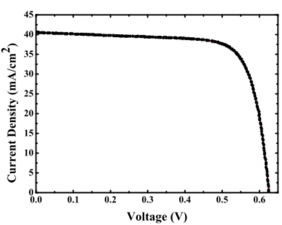
Abstract: n-type silicon shows the better tolerance towards metal impurities with a higher minority carrier lifetime compared
to p-type silicon substrate. Due to better lifetime stability as compared to p-type during illumination made the photovoltaic community to switch toward n-type wafers for high efficiency silicon solar cells. We fabricated the front electrode of the n-type solar cell with AgAl paste. The electrodes characteristics of the AgAl paste depend on the contact junction depth that is closely related to the firing temperature. Metal contact depth with p+ emitter, with optimized depth is important as it influence the resistance. In this study, we optimize the firing condition for the effective formation of the metal depth by varying the firing condition. The firing was carried out at temperatures below 670℃ with low contact depth and high
contact resistance. It was noted that the contact resistance was reduced with the increase of firing temperature. The contact resistance of 5.99 mΩ㎠ was shown for the optimum firing temperature of 865℃
. Over 900℃
, contact junction is bonded to the Si through the emitter, resulting the contact resistance to shunt. we obtained photovoltaic parameter such as fill factor of 76.68%, short-circuit current of 40.2 mA/cm2, open-circuit voltage of 620 mV and convert efficiency of 19.11%.Keywords: Screen printing, N-type solar cells, Metallization, Contact resistivity(ρ
c), AgAl electrode1. 서 론
a. Corresponding author; [email protected] Copyright ©2016 KIEEME. All rights reserved.
This is an Open-Access article distributed under the terms of the Creative Commons Attribution Non-Commercial License (http://creativecommons.org/licenses/by-nc/3.0) which permits unrestricted non-commercial use, distribution, and reproduction in any medium, provided the original work is properly cited.
최근 실리콘 태양전지에 전극을 형성하기 위하여 가
장 광범위하게 이용하는 공정은 크게 스크린 인쇄법
(screen print method)과 소성 공정(firing process)
으로 분류된다 [1-3]. 스크린 인쇄법은 사진 평판술
(photolithography technology), 매립형 접촉술
(buried contact technology), 도금(plating) 및 금속
스퍼터(metal sputter)와는 다르게 공정이 간단하고, 시 간을 절약할 수 있으며, 비용이 경제적이다. 그리고 환 경에 영향을 거의 주지 않기 때문에 화학폐기물을 줄일 수 있고, 비교적 친환경적인 기법이다 [4]. 이러한 방법으 로 고효율 태양전지를 제조하기 위해, 스크린 인쇄 공정과 소성 조건, 페이스트 등 이와 같은 변수를 신중하게 제어할 필요가 있다. 금속화 공정(metallization process)은 충진율 (fill factor), 병렬저항(shunt resistance), 직렬저항(series resistance), 개방전압(open-circuit voltage) 및 단락전류 (short-circuit current)와 같은 태양전지의 다양한 특성에 강하게 영향을 준다. 소성 공정을 진행하는 동안에 도핑의 농도나 깊이 및 페이스트에 의한 영향을 받을 수 있기 때 문에 소성 조건을 제어하는 것은 중요하다 [5].
페이스트는 크게 고온 소성 페이스트와 저온 경화 페 이스트로 분류할 수 있으며, 각각 결정질 태양전지와 실 리콘 이종접합 (SHJ) 태양전지의 전극을 형성하기 위해 사용한다. 일반적으로 Ag 고온 소성 페이스트의 경우 총 4개의 소성단계를 분류할 수 있다. 첫 번째 단계 550℃ 이하에서는 유기물과 용제가 완전히 분해되어 반 응이 일어나고, Ag 입자의 소결반응과 glass frit의 감 소가 시작된다. 두 번째 단계 550℃ ~ 700℃에서는 glass frit의 감소량이 증가하며, passivation layer와 Ag 사이에서 액체를 형성하고, passivation layer를 뚫 고 들어가기 시작한다. 세 번째 단계 700℃ ~ 800℃는 passivation layer가 완벽하게 뚫리며, PbO layer와 Si 사이에서 산화환원 반응이 일어나 Ag 결정화가 이루어 진다. 네 번째 단계는 cooling down으로 Ag와 Pb의 분리가 일어나며, Ag의 재결정화로 인한 전극이 형성된 다. AgAl 페이스트는 일반 Ag 페이스트와 달리 Al이 첨가되어 낮은 접촉저항의 전극을 형성할 수 있다는 장 점이 있는 반면에 소성 과정에서 deep metal spike로 인하여 에미터가 쉽게 관통된다는 단점이 있다.
본 실험에서는 80 Ω/□의 고정된 에미터 위에 고온 소성 AgAl 페이스트를 인쇄하여 최적의 접촉저항을 얻 기 위하여 소성 조건의 영향을 연구하였다. 벨트형 소성 로 4개의 영역 온도를 설정하였고, 벨트 속도를 변경하 여 소성 과정에서의 최대 온도 상승 속도를 조정하였다.
2. 실험 방법
본 실험에서는 고온 소성 AgAl 페이스트의 최적화 된 접촉 비저항(contact resistivity)을 얻기 위하여, 소성 온도와 벨트 속도를 가변하며 소성 프로파일의
Table 1. Screen printer settings.
Model name MT-550TV
Squeegee Pressure (MPa) 0.200
Squeegee Speed (mm/sec) 60
Scrubber Pressure (MPa) 0.100
Scrubber Speed (mm/sec) 40
Snap off Distance (mm) 1.25
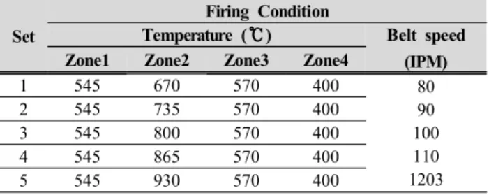
Table 2. High temperature firing condition for obtaining specific contact resistivity.
Set
Firing Condition
Temperature ( ℃) Belt speed (IPM)
Zone1 Zone2 Zone3 Zone4
1 545 670 570 400 80
90 100 110 1203
2 545 735 570 400
3 545 800 570 400
4 545 865 570 400
5 545 930 570 400
최적화 방법과 소성 과정에서 발생하는 substrate과 paste 간의 결합이 소자에 미치는 영향을 연구하였다.
비저항 1 ~ 2 Ωcm, 두께 200 ㎛의 태양전지급 쵸크 랄스키법 N-형 실리콘 단결정 웨이퍼를 사용하였다 [6]. (NaOH 8%+TCL 0.5%)의 혼합용액에서 10분간 Saw damage를 제거하였으며, (NaOH 2%+IPA 12.5%+Na
2SiO
318%)의 혼합용액으로 random pyramid texture 공정을 40분간 진행하여 small size pyramid를 형성하였다. 이후 수평의 확산형 로에서 확 산 도핑 공정을 1,080℃-950℃-850℃-750℃ 단계로 총 20분간 진행하였으며, 80 Ω/□의 에미터 Boron tribromide (BBr
3)를 도핑하였다. 스크린 프린터 (MT-550TV, Microtec)를 사용하여 전면 에미터 위에 전달 길이 분석법 (transmission length method, TLM) 패턴을 인쇄하였으며, 온도 150℃에서 4분간 건 조 공정 및 고온 소성 공정을 거쳐 전극을 형성하였다.
표 1은 실험 진행을 위해 사용한 스크린 프린터의 설정 값이다.
표 2는 최적화된 접촉 비저항을 얻기 위한 소성로의 조건을 나타내고 있다. Zone 2 외의 3개의 zone의 온 도는 고정하였으며, 벨트 속도를 변화하여 최대 온도와 소성 시간을 조정하였다 [7,8].
소성 조건 온도와 벨트속도의 변화에 따른 접촉 비
저항을 분석하기 위하여 전달 길이 분석법을 이용하여
진행하였다. 소성 조건에 따른 표면 형상의 변화를 관
찰하기 위하여 전자주사현미경 (JEOL-7600F,
scanning electron microscope, SEM)을 사용하여 촬영 및 분석하였다.
3. 결과 및 고찰
Table 3. Specific contact resistivity, as temperature and belt speed varied in various firing conditions.
Experiment result Temperature
(℃) 670 735 800 865 930
Contact resistivity
(mΩcm
2)
181.82 13.70 15.28 5.99 26.23
IPM 80 90 100 110 120
Contact resistivity
(mΩcm
2)
9.36 8.71 7.26 5.99 14.78
600 700 800 900 1000
0 3 6 9 0 3 6 9 40 60 80 0 20 40 60
Component Weight (%)
Firing Temperature (℃) O Al Si Ag
Fig. 1. Component atomic ratio at various firing temperatures.
표 3은 소성 온도와 벨트 속도의 변화에 따른 접촉 비저항 측정 결과를 나타낸다.
그림 1은 소성 온도의 변화에 따른 접촉 비저항과 AgAl 전극의 구성 원자 비율을 나타낸다. 소성 온도가 670℃에서 935℃까지 변화함에 따라 Al의 원자 비율은 감소하고, Ag의 원자 비율은 증가한다. 이는 온도가 증 가할수록, AgAl 페이스트와 Si 사이에서 산화환원 반 응이 발생하여, Ag와 Al이 Si층을 파고들어 결정화가 진행되기 때문이다. 이러한 결과로 소성 온도 865℃에 서 5.99 mΩcm
2의 접촉 비저항이 측정되었다 [9,10].
600 700 800 900 1000
0 10 20 0 3 6 9 50 60 70 80 90 0 10 20 30
Component Atomic (%)
Firing Temperature (℃) O Al Si Ag
Fig. 2. Component weight ratio at various firing temperatures.
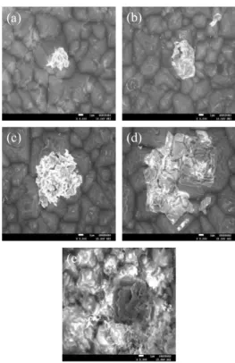
(a) (b)
(c) (d)
(e)
Fig. 3. FE-SEM images of AgAl paste contact point on substrate surface at various firing temperatures. (a) 660℃, (b) 735℃, (c) 800℃, (d) 865℃, and (e) 930℃.
그림 2는 소성 온도의 변화에 따른 접촉 비저항 및
AgAl 전극의 구성 성분의 중량을 나타낸다. 소성 온도
가 증가할수록, Ag의 중량이 증가하는 것을 확인할 수
0.0 0.1 0.2 0.3 0.4 0.5 0.6 0
5 10 15 20 25 30 35 40 45
Current Density (mA/cm2 )