High-quality ZnO nanowire arrays directly synthesized from Zn vapor depo- sition without catalyst
Tran Van Khai, Maneeratanasarn Prachuporn, Bong Geun Choi, Hyoun Woo Kim, Dae-Sup So*, Joon Woo Lee*, No-Hyung Park**, Hoon Huh**, Ngo Trinh Tung***,Heon Ham and Kwang Bo Shim† Division of Advanced Materials Science Engineering, Hanyang University, Seoul 133-791, Korea
*National Nanotechnology Policy Center, Korea Institute of Science and Technology Information, Seoul 130-741, Korea
**Korea Institute of Industrial Technology, Cheonan 331-825, Korea
***Institute of Chemistry, Vietnam Academy of Science and Technology (VAST), 18 Hoang Quoc Viet, Caugiay, Hanoi, Viet Nam (Received June 7, 2011)
(Revised July 27, 2011) (Accepted July 29, 2011)
Abstract Vertically well-aligned ZnO nanowire (NW) arrays were synthesized directly on GaN/sapphire and Si substrate from Zn vapor deposition without catalysts. Experimental results showed that the number density, diameter, crystallinity and degree of the alignment of ZnO NWs depended strongly on both the substrate position and kind of the substrates used for the growth. The photoluminescence (PL) characteristics of the grown ZnO NW arrays exhibit a strong and sharp ultraviolet (UV) emission at 379 nm and a broad weak emission in the visible range, indicating that the obtained ZnO NWs have a high crystal quality with excellent optical properties. The as-grown ZnO NWs were characterized by using scanning electron microscopy (SEM), high resolution transmission electronic microscopy (HR-TEM), and X-ray diffraction (XRD).
Key words ZnO nanostructures, Nanowire, GaN, ZnO photoluminescence
1. Introduction
In recent years, one-dimensional (1D) semiconductor nanostructures, such as nanowires (NWs) [1], nanorods (NRs) [2], nanobelts and nanotubes [3, 4], have attracted tremendous attention due to their unique properties and potential applications. Among the various 1D semicon- ductor materials, ZnO NWs have been widely studied.
ZnO is a wide direct band-gap (3.37 eV) semiconductor material, high electron mobility, high thermal conductiv- ity and mechanical strength, with a large exciton bind- ing energy (60 meV), which is much larger than that of GaN (25 meV) and the thermal energy (26 meV), so that excitionic emission processes can persist at or even above room temperature [5]. All these features make ZnO material an outstanding candidate for visible, ultraviolet light-emitting diodes (LEDs) and lasers [6], and thus are promising to compete with GaN-based ones for next- generation data-storage lasers [7].
Recently, special attention has been paid to the impor- tance of vertically well-aligned ZnO NW arrays, in both the fundamental physical science and potential applica- tions. Vertically well-aligned ZnO NW arrays can effec-
tively transport electrons and photons, and are considered to be promising building blocks for a wide range of novel optical or optoelectronic nanodevices. Recently, the advan- tages of vertically well-aligned ZnO NW arrays not only can be realized, but also may be enhanced due to their homogenous behaviour. From the application point of view, the diameter, density, morphology and uniform dis- tribution of well-aligned ZnO NWs are of very impor- tant issues since they can directly influence the optical, electrical, and mechanical properties in devices [8, 9].
Therefore, the control growth of vertically well-aligned ZnO NW arrays with optimal density and diameter will be important and indispensable from practical applications.
Until now, the only method of tuning the oriented growth, diameter and density of ZnO NWs/NRs is to mod- ify the size of catalyst particle and the thickness of the metal catalyst films [10, 11]. However, unfortunately, the catalysts can be easily remained in the final ZnO nano- structure, resulting in unfavourable properties. Therefore, the remaining catalyst or additives should be completely removed from the grown ZnO NWs. On the other hand, it was found that the alignment of ZnO NW arrays was due to not only experimental conditions but more impor- tantly the epitaxial orientation relationship with the sub- strate. The matching in lattice parameters and the crystal structure between ZnO and substrate strongly affected the crystal growth behaviour and thus, result in changes
†Corresponding author
†Tel: +82-2-2299-2043
†Fax: +82-2-2281-4133
†E-mail: [email protected]
in the degree of alignment of ZnO NWs. Therefore, the suitable substrate selection is a very important issue for the growth of vertically well-aligned NW arrays. Up to now, it is not easy to directly grow and control the align- ment, density as well as diameter of ZnO NW arrays by the thermal evaporation method without the use of cata- lysts; this method was usually employed to synthesize disarrayed nanostructures [12].
In this study, we show that vertically well-aligned ZnO NW arrays can be directly synthesized on the GaN/sap- phire and Si substrate by a simple thermal evaporation method. The influences of the distance between Zn source and substrate on the growth behaviour of the ZnO NW arrays, such as the density, vertical alignment, average diameter, crystallinity and defect density are investigated.
In addition, we will show the important role of GaN epilayer in epitaxial growth of vertically aligned NW arrays. Moreover, the structural and optical properties of the obtained ZnO NW arrays will also be studied in detail.
2. Experiment
The synthesis of ZnO NWs was carried out using a conventional horizontal quartz tube furnace with inner diameter of 20 mm and was composed of two heating zone of 300 mm. The un-doped GaN epilayers were grown on c-sapphire substrate by the hydride vapor phase epitaxy (HVPE) technique [13] were used for deposition of the NWs. Before loading the Si and GaN/
sapphire (0.5 × 0.5 cm
2) substrates in the reactor, they were etched with H
3PO
4(80 %) solution for 1 minute to remove the native oxide layer and then keenly washed with acetone, methanol and de-ionized water, and finally dried by air. The substrates were put on the top of an alumina boat loaded with high purity metallic zinc pow- der (75
µm, 99.99 %, Japan) about 0.25 g, were insertedinto the center of the furnace. The vertical distance between the zinc source and substrate was about 5 mm, with a downstream separation of 5~25 mm. The fur- nace was heated to the reaction temperature of 620
oC in 30 min under Ar at a flow rate of 350 standard cubic centimeter mass (sccm). The zinc source was thermally vaporized to synthesize ZnO NWs at atmospheres pres- sure under Ar (99.999 %) at a flow rate of 350 sccm for 90 min at 620
oC. After reaction, the quart tube was cooled to room temperature under Ar at a flow rate of 100 sccm. The substrate surface appeared to be a layer of white wax-like material.
The morphology of the ZnO NWs was examined by a scanning electron microscope (SEM, JEOL, JSM 5900 LV, Japan). The crystal structure was identified by means X-ray diffraction (XRD, Cu K
α wavelength at 1.54 Å,40 kv, 30 mA, Rigaku, Japan). The crystallinity of a sin- gle ZnO NW was investigated by transmission electron microscope (TEM, JEOL, JEM-4010, 400 kv, point-to- point resolution is 0.15 nm, Japan). The photolumines- cence (PL) measurements were performed using the 325 nm line of He-Cd laser as the excitation source with a 350 nm filter.
3. Results and Discussion
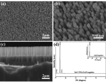
Fig. 1(a~c) show typical SEM images of the ZnO NW arrays grown on the GaN/sapphire substrate from Zn vapor deposition without a catalyst. From Fig. 3, the distance between Zn source and GaN/sapphire substrate is about 7 mm. As shown in Fig. 1a, it was found that almost the entire surface of the substrate is uniformly covered with vertically well-aligned ZnO NW arrays, even on the sides of the substrate. A higher magnifica- tion SEM image, in Fig. 1b, clearly shows that all of the ZnO NWs are straight and well-aligned in a direction normal to the substrate surface. Most of these NWs have a clean surface and a faceted hexagonal shape. The hexagonal shape of the NWs points out that the NWs grew epitaxially on the GaN layer/sapphire substrate [14].
Structurally, it is know that the ZnO and GaN have the same type of crystal structure and a small mismatch of
Fig. 1. (a) Low and (b) high-magnification tilted-view SEM images; (c) Cross-sectional SEM image; and (d) XRD pattern of vertically aligned ZnO NW arrays formed on GaN/sapphire substrate without a catalyst. The inset in (d) shows the XRD
pattern of GaN layer/sapphire substrate.
lattice constants (~1.8 %) [15]; these advantages make GaN suitable for epitaxial growth of ZnO nanostructures [16]. It was shown that perfect vertically aligned ZnO NW arrays can only occur on GaN(0001) and SiC(0001) substrates due to reduced lattice mismatch [17, 18]. This suggested that the small lattice mismatch between the NWs and substrates is believed to play a very important role in epitaxial growth of vertically well-aligned arrays.
As shown in Fig. 1(b), it is clearly seen that there are two typical diameters among those NWs. The majority of those NWs are individual wires, which have diame- ters about 120~150 nm, and the other NWs with diame- ters are in the range of 200~250 nm which can be due to the combination of two thinner NWs [19, 20]. How- ever, those NWs have a highly uniform diameter along their lengths, as shown in Fig. 1(c). In addition, the length of the NWs has also a uniform distribution, and it is approximately 3
µm.Fig. 1(d) shows the XRD pattern of the ZnO NWs and the inset in (d) shows the pattern of the GaN/sap- phire substrate. From the pattern of the GaN/sapphire substrate, it is found that the GaN buffer layer is single crystal with hexagonal wurtzite structure. Only the GaN(002) peak appears in the X-ray spectrum, indicat- ing that the GaN layer is well c-oriented. For the as- grown ZnO NWs, although there are some weak extra (100) and (101) peaks in the spectrum, the ZnO(002) peak is very sharp and intensity of its is much higher than any other peaks, including the substrate peak. This indicates that the crystalline quality of the ZnO NW has been dramatically improved in comparison with that of bulk ZnO powder. All diffraction peaks in this pattern are well matched with the hexagonal wurtite structure of single-crystalline ZnO phase with lattice constants of a = 3.256 A
oand c = 5.218 A
o, which are in good agreement with the standard value bulk hexagonal ZnO (JCDPDS No 05-0664: a = 3.249 A
oand c = 5.205 A
o). It can be concluded that the synthesized ZnO NW arrays are sin- gle crystalline with the hexagonal wurtzite phase and grown along the [001] direction with their c-axis per- pendicular to the substrate. No trace of zinc, impurity, or substrate is detected from the spectrum, confirming that the ZnO NWs sample is pure hexagonal ZnO. Based on the results from the X-ray analysis, it seems that the vertically well-aligned ZnO NW arrays are in perfect epitaxial relationship with the GaN layer. The high crystal quality of the GaN layer results in a good orientation of the nanostructures and hence the ZnO NW arrays are also grown epitaxially along the same direction. The similar result was found in the previous paper [21], in
which it showed that a buffer layer was used as sub- strate to control the growth direction of the 1-D ZnO nanostructures. Hence, it can be concluded that the GaN layer is the key factor that helps oriented growth and improvement of crystal quality of the ZnO NWs. Further investigations for the influence of the quality of GaN buffer layer such as the thickness, grain size, surface, etc., on the synthesis of ZnO NWs are underway and will be reported elsewhere.
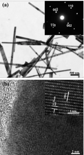
The detailed structural characterization of the as- grown ZnO NWs was investigated with TEM. Fig. 2a
Fig. 2. TEM images of ZnO NWs grown at distance of (l = 7 cm) from the zinc source: (a) Low-resolution TEM; The inset shows the corresponding SAED pattern. (b) High-resolution TEM image of a single-crystalline ZnO NW showing the lat- tice fringes; The inset is a magnified image of the single ZnO NW with the lattice spacing of 0.26 nm between adjacent lat- tice planes, indicating that the NW grown along the [001]
direction.
shows several the NWs, which were scratched from the ZnO NWs grown on the GaN/sapphire. It indicates that the NWs have a straight shape and uniform diameter along their length; most of them are 100~180 nm in diameter, although some large wires (~250 nm) are also observed. Unlike the metal catalyst assisted process, no catalyst particles can be observed at the top or bottom of the wire.
The inset in Fig. 2(a) displays the selected-area elec- tron diffraction (SAED) pattern, which further provides evidence of the oriented growth of the ZnO NWs on GaN/shappire substrate. It reveals that the ZnO NW has a single-crystal wurtzite structure and c-axis orientation.
Fig. 2b shows high-resolution TEM image of a single ZnO NW. It is found that the ZnO NW has a clean sur- face, contains no defects such as dislocation and stacking faults, no amorphous layer on the surface was observed in the HR-TEM, which implies that it has no contami- nation and was synthesized with excellent quality. The inset in Fig. 2(b) is the lattice-resolved HR-TEM image of a segment of a single ZnO NW. It is seen clearly that the ZnO crystal lattices are well-oriented with no observ- able structural defects in the whole regions. This result indicates that the obtained ZnO NWs are structurally homogeneous and defect-free. The lattice spacing of the as-grown ZnO NW is about 0.26 nm between adjacent lattice planes, corresponding to the distance between two (002) crystal planes, which confirms that the as-grown ZnO NWs are highly preferential growth along the [001]
direction.
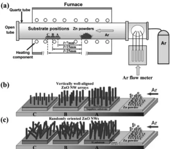
To understand the influence of substrate position on the growth behaviour of ZnO NWs on the GaN/sapphire, the NW samples were synthesized at different substrate positions with the other growth conditions fixed. Three pieces of the GaN layer/sapphire substrates were placed at positions ‘A’, ‘B’, and ‘C’, corresponding to the dis- tances (l) between Zn source and substrate are 7, 15, and 25 mm, as illustrated in Fig. 3(a). Fig. 3(b & c) show a sketch for the growth of vertically well-aligned ZnO NW arrays on GaN/sapphire and Si substrate at different substrate positions, respectively. We found that the growth behaviour of the ZnO NW arrays on the sub- strate was very sensitive to the distance (l) and can be definitely controlled by adjusting the substrate position with respect to the source materials. It was observed that the number density, diameter and length of the ZnO NW arrays gradually decreased with increasing the dis- tance (l). Fig. 4(a~c) shows the growth behaviour of the ZnO NWs on the GaN/sapphire substrate at different substrate positions. It is clearly found that the vertically
well-aligned ZnO NW arrays were grown on all the substrate positions. Although there were variations in the diameter and lengths of the NWs with the distance
Fig. 4. Tilted-view SEM images of the grown ZnO NWs depending on the substrate positions: (a~c) well-aligned ZnO NW arrays grown on GaN/sapphire; (d~e) ZnO NWs grown onSi substrate at position ‘A’, ‘B’ and ‘C’, respectively.
Fig. 3. (a) A schematic diagram of the experimental apparatus for the growth of vertically well-aligned ZnO NW arrays. The substrate positions ‘A’, ‘B’ and ‘C’ are distance from the zinc source, corresponding to the distance (l): ‘A’ = 7 mm, ‘B’ = 15 mm, and ‘C’ = 25 mm. (b), (c) A sketch for the ZnO NW arrays
growth on different substrate positions.
(l), all the NWs were well aligned in a direction perpen- dicular to the substrate surface. Regardless of the sub- strate position, there were no significant changes in the degree of vertical alignment of the NWs. Many ZnO NWs and NRs were prepared by the same method;
however, had been grown with random orientations [1, 22], even with regard to the substrate position [23]. The result suggested that the origin of the vertical alignment can be ascribed to preferential orientation of the GaN layer, in which most of (002) planes are parallel to the GaN/sapphire interface.
For the purpose of comparison, Fig. 4(d~f) show typi- cal SEM images of the ZnO NWs grow directly on the Si substrates with the same growth conditions above.
Clearly, it was seen that the degree of alignment of the ZnO NWs strongly depended on the substrate position.
The NWs were also observed at all substrate positions;
however, the alignment of the NWs was gradually de- creased as the distance (l) was increased. This observa- tion shows that the growth behaviour of the ZnO NWs on the Si substrate is quite different from that of the ZnO NWs on the GaN/sapphire substrate. The reason can be attributed to the large differences in their thermal expansion coefficients, lattice mismatch and difference in crystal structure cause a rather large stress between ZnO and Si substrate [24, 25]. On the other hand, it was found that, due to higher rate of nucleation on the Si substrate, the surface density of nucleation centres was very high [26] and incompatibility of the lattice structure between the cubic Si substrate and the hexagonal ZnO.
As a result, this led to formation of less-aligned ZnO NWs and randomly oriented on the Si substrate [27]. Moreover, the Si surface readily got oxidized during the nucleation stage of the ZnO growth process via thermal evaporation method, in which these oxides were an amorphous film without crystal orientation [43]. Consequently, this could lead to the growth of randomly oriented ZnO NWs along the in-plane direction [21]. Therefore, it can be not easy to obtain well aligned ZnO NWs and uniformly oriented in the in-plane direction of the Si substrate. In spite of variation in the degree of the alignment, however it was usually observed that the number density and the growth rate of the ZnO NWs on the Si substrate were higher than that of on the GaN/sapphire substrate. Further and more detailed investigations using more sensitive tech- niques are necessary to determine it carefully.
It was also observed that not only the degree of align- ment but also the morphology ZnO nanostructures were very sensitive to the substrate poison and the growth temperature [29, 30]. Therefore, optimizing experimen-
tal parameters in the system is extremely crucial for the formation of a specific type of morphology, and in determining the degree of the vertical alignment. In this study, due to the temperature gradient, the substrate tem- perature was found to be dependent on its position. Our experimental results showed that in a substrate tempera- ture range of 580~620
oC, only ZnO NWs were observed.
The similar result also reported in the previous study [31], in which that indicated that the substrate temperature greatly influenced the morphology of ZnO nanostructures synthesized by the thermal evaporation process. There- fore, it can be concluded that the control of the substrate temperature is key issue in the synthesis of nanostruc- tured ZnO with a particular shape [3]. Of course, the morphology of the deposited products can be controlled by varying the other experimental parameters, was reported elsewhere [32]. Based on above results, it can be con- cluded that the alignment of the ZnO NWs greatly de- pended on not only the type of the substrates used for the growth, but also on the substrate position. Therefore, the introduction of the GaN layer with preferred orienta- tion as a template layer will be very useful in manufac- turing 1D ZnO NWs with a high quality, a vertical alignment, and large-scale production. Additionally, adjust- ing the substrate position was found to be a key factor for the formation ZnO nanostructure with a particular kind of morphology and control of the degree of align- ment.
The crystallinity and degree of vertical alignment of as-grown ZnO NWs on GaN/sapphire and Si substrate at different position were examined using XRD. Fig. 5(a
& b) show the XRD patterns for the ZnO NWs grown on GaN/sapphire and Si substrate at position ‘A’, ‘B’
and ‘C’, respectively. All the indexed peaks shown in all
the spectra are well matched with wurtzite hexagonal
phase of the ZnO bulk. No other impurity or substrate
peaks were observed in the spectra, indicating that the
NWs obtained are only hexagonal ZnO. For the ZnO
NWs on the GaN/sapphire, in all the spectra, the inten-
sity of the (002) peak is very sharp and strong com-
pared with those of the other peaks, indicating that all
the ZnO NW arrays are highly preferential growth along
the c-axis direction and perpendicular to the substrate
surface. Unlike in the case of the ZnO NWs grown on
the GaN/sapphire, the (002) peak intensity of the ZnO
NWs grown on Si substrate is significantly reduced, and
it is around fifteen times smaller than that of the ZnO
NWs on the GaN/sapphire. It implies that the crystal
quality of the ZnO NWs grown on Si substrate was not
as good as that of the ZnO NWs grown on the GaN/
sapphire substrate. Besides the (100), (002) and (004) peaks, like in the case of ZnO NWs grown on the GaN/
sapphire, also includes other diffraction peaks, such as the (102), (103), (200), (112), and (201), etc., are simul- taneously observed since the NWs were directly synthe- sized on the Si substrate. This indicates that the ZnO NWs directly grown on Si substrate are randomly ori- ented in the in-plane direction. In all cases, the intensity
and sharpness of the (002) peak increase dramatically with shortening the distance (l), indicating that higher substrate temperature leads better crystallinity of ZnO NWs. From XRD results, we obverse that the NWs grown at position ‘A’ have the highest (002) peak intensity, confirming that these NWs have best c-axis-oriented structure and possess the best crystalline quality, com- pared with the NWs grown at position ‘B’ and ‘C’.
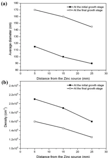
Fig. 6 shows the change of diameter and density of the NWs with the substrate position. Detailed analysis of the SEM images (not shown here) reveals that the density of the NWs at the initial growth stage (for 1 min) are estimated to be 2.1 × 10
9, 1.8 × 10
9, and 1.6 × 10
9/ cm
2, and their average diameter: 115, 100 and 90 nm, corresponding to the substrate placed at position ‘A’, ‘B’
and ‘C’, respectively. After 90 min growth, the density and average diameter of final ZnO NWs are estimated to be 1.6 × 10
9, 1.45 × 10
9cm
−2and 1.25 × 10
9cm
−2, and 170, 160 and 145 nm, corresponding to the substrate placed at position ‘A’, ‘B’ and ‘C’, respectively. It is
Fig. 5. XDR patterns of the grown ZnO NWs on (a) GaN/sap-phire and on (b) Si substrates at position ‘A’, ‘B’ and ‘C’, respectively.
Fig. 6. The change of average diameter and density of the NWs at the initial and final growth stage, both changes in the
diameter and density depending on the substrate positions.
interesting to note that although there are variations in the diameter size and density of the final NWs on each substrate position, the diameter and density distribution of which relatively correspond to that of the ZnO NWs at the initial growth stage. This implies that the control of the size and density of the NWs at the initial growth stage plays important role in determining both the num- ber density and diameter of the final NWs. In the present case, the size and density ZnO seeds can be controlled by adjusting the substrate position. At present we believe that the change of the substrate position can result in change in the amount of Zn vapor source, and conse- quently change in the density and diameter size of the final ZnO NWs. It is assumed that the mount of Zn vapor source gradually decreases as the distance between Zn source and substrate increases, resulting in both the density and NW diameter reduce to compensate for lack of the vapour [33]. It was also reported that the zinc vapor pressure decreased as the distance between the zinc source and the substrate increased [34]. Moreover, the variation in the substrate position may affect both the vapor pressure and concentration of the source mate- rial [35]. Therefore, as the distance (l) increases, the vapor pressure and concentration of the zinc source decrease, resulting in the decrease in the diameter size and density of the NWs. From these results, it can be concluded that vertically well-aligned ZnO NW arrays with the highly desirable properties could be achieved by optimal selection of the appropriate substrate position.
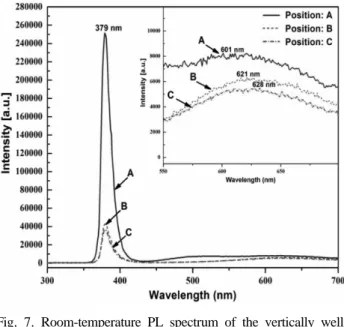
Fig. 7 shows the PL spectra of the as-grown NWs on GaN/sapphire substrates at different substrate position
were measured at room temperature. The strong and sharp ultraviolet (UV) emission peak centered at 379 nm was observed for all the NWs samples regardless of the sub- strate position. This wavelength corresponds to the ban gap energy of 3.27 eV of ZnO material. Regarding the appearance of the visible emission peaks, it is observed that there are some differences in PL properties among these samples. In addition to the UV emission peak, a very weak and broad green and orange emission peaks centered at 535 nm and 601 nm, respectively, can be observed from the ZnO NWs grown at position ‘A’.
However, the green emission peak is not observed, while the orange emission at 601 nm is red-shifted to 621 nm and 628 nm is found in the PL spectra of ZnO NWs grown at position ‘B’ and ‘C’, respectively. Cur- rently, the UV emission has been clearly understood as the near-band edge (NBE) emission of wide direct band- gap of ZnO which is originated from the recombination of free-exciton through an exciton-exciton collision pro- cess [36]. Meanwhile, the green, orange and red emission peaks, known as deep-level emission (DLE), they are usually considered to be related to the extrinsic impuri- ties [37] and intrinsic structural defects in the ZnO crystal lattice, such as oxygen vacancy (Vo) [38], oxide antisite defect (O
Zn) [39], oxygen interstitials (O
i) [40], zinc interstitials (Zn
i) [41] and Zn vacancy (V
Zn) [42]. How- ever, due to its sensitivity to the crystallization, struc- tural disorders and defects in the nanostructures, as well as the complexity of the microstructure of ZnO, the exact origin of the visible emissions in ZnO is not yet well understood and is still controversial.
It was also generally accepted that the surface states play a very important role in the PL spectra of nanoma- terials [43]. Regarding the origination of green emission, Vanheusden et al [38] supposed that it originates due to the radial recombination of a photon generated hole with an electron that belongs to a singly ionized oxygen vacancy in the surface and sub-surface lattices of the ZnO mate- rial [44] (dominant in bulk ZnO) and recombination at surface states (low dimensional structures with high vol- ume to surface ratio) [45]. Meanwhile, the orange and red emissions had been suggested mainly due to the intrin- sic defects in ZnO, especially oxygen interstitials (O
i) created by excess oxygen are main cause [46] and per- haps had much to do with the structure of ZnO
x[47]. In our case, all the ZnO NWs exhibited a suppressed and weak visible emission, indicating that the as-grown ZnO NWs have very few structural defects regardless of the substrate position.
It was believed that the diameter size of NWs could
Fig. 7. Room-temperature PL spectrum of the vertically well-aligned ZnO NW arrays grown at the position ‘A’, ‘B’ and ‘C’.
affect the difference of emission intensity [1]. In the present case, it is clearly seen that the intensity of the free-exciton emission (I
UV) increases prominently with the diameter NWs. Owing to a smaller surface-to-volume ratio; the larger diameter has less substantial non-radia- tive relaxation occurring through the surface states, which significantly enhances the excitons emission process and hence increases I
UV. The sample at position ‘A’, with highest intensity of (002) peak and largest diameter, has the best PL property. Hence the UV emission was found to be size-dependent and crystal orientations of the NWs [48]. On the other hand, it was found that the density of NWs could also affect the emission intensity [49]. As the mount and density of stoichiometry of ZnO NWs increase, those result in the increase of PL intensity [50]. As estimated by SEM observations, the total mass of the ZnO NWs at position ‘A’ is roughly higher than that at position ‘B’ and ‘C’. Consequently the increase of I
DLEof the sample grown at ‘A’ can be attributed to an increase amount of structural defects due to higher density. However, the intensity ratio of the UV emis- sion to the deep-level emission in the NWs at position
‘A’ (I
UV/I
DLE= 30.5) is much larger than that of the NWs at position ‘B’ (I
UV/I
DLE= 6.76) and ‘C’ (I
UV/I
DLE= 6.50), which indicates there are less structural defects for sam- ples grown at position ‘A’. From these results it can be concluded that the substrate position plays an important role in determining the type and concentration of defects in the ZnO NWs.
4. Conclusions
Vertically well-aligned ZnO NW arrays were success- fully synthesized on the GaN/sapphire and Si substrate via a simple thermal evaporation method by using metal- lic zinc powder without catalyst or additives. The as- synthesized ZnO NWs had diameters in the range of 100~240 nm and lengths of 3
µm. The vertical align-ment, number density, diameter, crystallinity, and defect density of ZnO NW arrays were found to be greatly dependent on the substrate position. In addition, it was also found that the kind of the substrate used for the growth was a key factor for the formation of vertically well-aligned ZnO NWs arrays in the large-scale area.
The HR-TEM, XRD and SAED measurements revealed that the ZnO NWs were single crystals and well ori- ented along the c-axis, with high crystalline quality. The PL spectra at room temperature showed that the as-grown ZnO NW arrays had excellent optical properties. It could
be concluded that by adjusting the substrate position and suitable substrate selection may be opened up opportuni- ties for fabricating 1D nanostructures with a high quality, a vertical alignment and a large-scale production.
References
[ 1 ] M.H. Huang, Y. Wu, H. Feick, N. Tran, E. Weber and P.
Yang, “Catalytic growth of zinc nanowires by vapor transport”, Adv. Mater. 13 (2001) 113.
[ 2 ] Z.L. Wang, “Zinc oxide nanostructures: growth, proper- ties and applications”, J. Phys.: Condens. Matter. 16 (2004) R829.
[ 3 ] Y.J. Xing, Z.H. Xi, Z.Q. Xue, X.D. Zhang, J.H. Song, R.M. Wang, J. Xu, Y. Song, S.L. Zhang and D.P. Yu,
“Optical properties of the ZnO nanotubes synthesized via vapor phase growth”, Appl. Phys. Lett. 83 (2003) 1689.
[ 4 ] J.J. Wu, S.C. Liu, T.C. Wu, K.H. Chen and L.C. Chen,
“Heterostructures of ZnO-Zn coaxial nanocables and ZnO nanotubes”, Appl. Phys. Lett. 81 (2002) 1312.
[ 5 ] D.M. Bagnall, Y.F. Chen, Z. Zhu, T. Yao, S. Koyama, M.Y. Shen and T. Goto, “Optically pumped lasing of ZnO at room temperature”, Appl. Phys. Lett. 70 (1997) 2230.
[ 6 ] A. Tsukazaki, A. Ohtomo, T. Onuma, M. Ohtani, T.
Makino, M. Sumiya, K. Ohtani, S.F. Chichibu, S. Fuke, Y. Segawa, H. Ohno, H. Koinuma and M. Kawasaki,
“Repeated temperature modulation epitaxy for p-type doping and light-emitting diode based on ZnO”, Nat.
Mater. 4 (2005) 42.
[ 7 ] M.H. Huang, S. Mao, H. Feick, H. Yan, Y. Wu, H.
Kind, E. Weber, R. Russo and P. Yang, “Room-tempera- ture ultraviolet nanowire nanolasers”, Science 292 (2001) 1897.
[ 8 ] S.H. Jo, J.Y. Lao, Z.F. Ren, R.A. Farrer, T. Baldacchini and J.T. Fourkas, “Field-emission studies on thin films of zinc oxide nanowires”, Appl. Phys. Lett. 83 (2003) 4821.
[ 9 ] Y.W. Zhu, H.Z. Zhang, X.C. Sun, S.Q. Feng, J. Xu, Q.
Zhao, B. Xiang and R.M. Wang, “Efficient field emis- sion from ZnO nanoneedle arrays”, Appl. Phys. Lett. 83 (2003) 144.
[10] P.D. Yang, H.Q. Yan, S. Mao, R. Russo, J. Johnson, R.
Saykally, N. Morris, J. Pham, R.R. He and H.J. Choi,
“Controlled growth of ZnO nanowires and their optical properties”, Adv. Funct. Mater. 12 (2002) 323.
[11] X.D. Wang, J.H. Song, C.J. Summers, J.H. Ryou, P. Li, R.D. Dupuis and Z.L. Wang, “Density-controlled growth of aligned ZnO nanowires sharing a common contact: A simple, low-cost, and mask-free technique for large- scale applications”, J. Phys. Chem. B 110 (2006) 7720.
[12] T.W. Kim, T. Kawazoe, S. Yamazaki, M. Ohtsu and T.
Sekiguchi, “Low-temperature orientation-selective growth and ultraviolet emission of single crystal ZnO nanow- ires”, Appl. Phys. Lett. 84 (2004) 3358.
[13] J.H. Ryu, D.K. Oh, S.T. Yoon, B.G. Choi, J.W. Yoon and K.B. Shim, “Optical characteristics of GaN single crystals grown by the HVPE: Effects of thermal anneal-
ing and N2 plasma treatment”, J. Cryst. Growth 292 (2006) 206.
[14] H.Q. Le, S.J. Chua, K.P. Loh, E.A. Fitzgerald and Y.W.
Koh, “Synthesis and optical properties of well aligned ZnO nanorods on GaN by hydrothermal synthesis”, Nanotechnology 17 (2006) 483.
[15] Y. Chen, D.M. Bagnall, H.J. Koh, K.T. Park, K.J.
Hiraga, Z. Zhu and T.J. Yao, “Plasma assisted molecu- lar beam epitaxy of ZnO on c-plane sapphire: Growth and characterization”, Appl. Phys. 84 (1998) 3912.
[16] H.J. Fan, B. Fuhrmann, R. Scholz, F. Syrowatka, A.
Dadgar, A. Krost and M. Zacharias, “Well-ordered ZnO nanowire arrays on GaN substrate fabricated via nano- sphere lithography”, J. Cryst. Growth 287 (2006) 34.
[17] B.H. Kong and H.K. Cho, “Growth and microstructural characterization of catalyst-free ZnO nanostructures grown on sapphire and GaN by thermal evaporation”, J. Mater.
Res. 22 (2007) 937.
[18] W.J. Mai, P.X. Gao, C.S. Lao, Z.L. Wang, A.K. Sood, D.L. Polla and M.B. Soporano, “Vertically aligned ZnO nanowire arrays on GaN and SiC substrates”, Chem.
Phys. Lett. 460 (2008) 253.
[19] C. Li, G. Fang, Q. Fu, F. Su, G. Li, X. Wu and X. Zhao,
“Effect of substrate temperature on the growth and pho- toluminescence properties of vertically aligned ZnO nanostructures”, J. Cryst. Growth 292 (2006) 19.
[20] L. Wang, X. Zhang, S. Zhao, G. Zhou, Y. Zhou and J.
Qi, “Synthesis of well-aligned ZnO nanowires by sim- ple physical vapor deposition on c-oriented ZnO thin films without catalysts or additives”, Appl. Phys. Lett.
86 (2005) 024108.
[21] H.M. Cheng, H.C. Hsu, S.Yang, C.Y. Wu, Y.C. Lee, L.J.
Lin and W.F. Hsieh, “The substrate effect on the in- plane orientation of vertically well-aligned ZnO nano- rods grown on ZnO buffer layers”, Nanotechnology 16 (2005) 2882.
[22] A. Umar, H.W. Ra, J.P. Jeong, E.K. Suh and Y.B. Hahn,
“Synthesis of ZnO nanowires on Si substrate by ther- mal evaporation method without catalyst: Structural and optical properties”, Korean J. Chem. Eng. 23 (2006) 499.
[23] U. Manzoor and D.Y. Kim, “Size control of ZnO nano- structures formed in different temperature zones by varying Ar flow rate with tunable optical properties”, Physica E 41(2009) 500.
[24] Y. Zhang, H. Jia and D. Yu, “Metal-catalyst-free epitax- ial growth of aligned ZnO nanowires on silicon wafers at low temperature”, J. Phys. D: Appl. Phys. 37 (2004) 413.
[25] H.C. Hsu, C.S. Cheng, C.C. Cheng, S. Yang, C.S. Chang and W.F. Hsieh, “Orientation enhanced growth and opti- cal properties of ZnO nanowires grown on porous sili- con substrates”, Nanochnology 16 (2005) 297.
[26] L. Vayssieres, “On the design of advanced metal oxide nanomaterials”, Int. J. Nanotechnol. 1 (2004) 1.
[27] J. Nayak, S.N. Sahu, J. Kasuya and S. Nozaki, “Effect of substrate on the structure and optical properties of ZnO nanorods”, J. Phys. D: Appl. Phys. 41 (2008) 115303.
[28] A. Nahhas, H.K. Kim and J. Blachere, “Epitaxial growth of ZnO films on Si substrates using an epitaxial GaN
buffer”, Appl. Phys. Lett. 78 (2001) 1511.
[29] S.C. Lyu, Y. Zhang, C.J. Lee, H. Ruh and H.J. Lee,
“Low-temperature growth of ZnO nanowire array by a simple physical vapor-deposition method”, Chem. Mater.
15 (2003) 3294.
[30] H. Tang, J.C. Chang, Y. Shan, D.D.D. Ma, T.Z. Lui, J.A. Zapien, C.S. Lee and S.T. Lee, “Growth mecha- nism of ZnO nanowires via direct Zn evaporation”, J.
Mater. Sci. 44 (2009) 563.
[31] Z.W. Pan, Z.R. Dai, L. Xu, S.T. Lee and Z.L. Wang,
“Temperature-controlled growth of silicon-based nano- structures by thermal evaporation of SiO powders”, J.
Phys. Chem. B 105 (2001) 2507.
[32] S.H. Dalal, D.L. Baptista, K.B. Teo and R.G. Lacerda,
“Controllable growth of vertically aligned zinc oxide nanowires using vapour deposition”, Nanotechnology 17 (2006) 4811.
[33] F. Fang, D.X. Zhao, J.Y. Zhang, D.Z. Shen, Y.M. Lu, X.W. Fan, B.H. Li and X.H. Wang, “The influence of growth temperature on ZnO nanowires”, Mater. Lett. 62 (2008) 1092.
[34] X.H. Han, G.Z. Wang, J.S. Jie, W.C. Choy, Y. Luo, T.I.
Yuk and J.G. Hou, “Controllable synthesis and optical properties of novel ZnO cone arrays via vapor transport at low temperature”, J. Phys. Chem. B 109 (2005) 2733.
[35] G. Shen and C. Lee, “CdS multipod-based structures through a thermal evaporation process”, Cryst. Growth
& Design 5 (2005) 1085.
[36] Y.C. Kong, D.P.Yu, B. Zhang, W. Fang and S.Q. Feng,
“Ultraviolet-emitting ZnO nanowires synthesized by a physical vapor deposition approach”, Appl. Phys. Lett.
78 (2001) 407.
[37] R. Dingle, “Luminsencent transitions associated with divalent copper impurities and the green emission from semiconductor Zinc oxide”, Phys. Rev. Lett. 23 (1969) 579.
[38] K. Vanheusden, W.L. Warren, C.H. Seager, D.R. Tal- lant, J.A. Voight and B.E. Gnade, “Mechanisms behind green photoluminescence in ZnO phosphor powders”, J.
Appl. Phys. 79 (1996) 7983.
[39] B.X. Lin, Z.X. Fu and Y.B. Jia, “Green luminescent center in undoped zinc oxide films deposited on silicon substrates”, Appl. Phys. Lett. 79 (2001) 943.
[40] Y. Yang, H. Yan, Fu Z, B. Yang, L. Xia, Y. Xu, J. Zuo and F. Li, “Photoluminescence and Raman studies of electrochemically as-grown and annealed ZnO films”, Solid State Commun. 138 (2006) 521.
[41] N.O. Korsumska, L.V. Borkovska, B.M. Bulakh, L.Y.
Knomenkava, V.I. Kushniranko and I.V. Markevich,
“The influence of defect drift in external electric field on green luminescence of ZnO single crystals”, J.
Lumin. 733 (2003) 102.
[42] A.F. Kohan, G. Ceder, D. Morgan and C.G. Van de Walle, “First-principles study of native point defects in ZnO”, Phys. Rev. B 61 (2000) 15019.
[43] K.Vanheusden, C.H. Seager, W.L. Warren, D.R. Tallant and J.A. Voigt, “Mechanisms behind green photolumi- nescence in ZnO phosphor powders”, Appl. Phys. Lett.
68 (1996) 403.
[44] A. Umar, B. Karunagaran, E.K. Suh and Y.B. Hahn,
“Structural and optical properties of single-crystalline
ZnO nanorods grown on silicon by thermal evapora- tion”, Nanotechnology 17 (2006) 4072.
[45] B.D. Yao, Y.F. Chen and N. Wang, “Formation of ZnO nanostructures by a simple way of thermal evapora- tion”, Appl. Phys. Lett. 81 (2002) 757.
[46] R. Calarco, R.J. Meijers, R.K. Debnath, T. Stoica, E.
Sutter and H. Lüth, “Nucleation and growth of GaN nanowires on Si(111) performed by molecular beam epi- taxy”, Nano Lett. 7 (2007) 2248.
[47] W.D. Yu, X.M. Li and X.D. Gao, “Effect of zinc sources on the morphology of ZnO nanostructures and their photoluminescence properties”, Appl. Phys. A 79 (2004) 453.
[48] A. Chatterjee, C.H. Shen, A. Granguly, L.C. Chen, C.W.
Hsu, J.Y. Hwang and K.H. Chen, “Strong room-temper- ature UV emission of nanocrystalline ZnO films derived from a polymeric solution”, Chem. Phys. Lett. 391 (2004) 278.
[49] K.A. Jeon, H.J. Son, C.E. Kim, J.H. Kim and S.Y. Lee,
“Photoluminescence of ZnO nanowires grown on sap- phire (1120) substrates”, Physica E 37 (2007) 222.
[50] H.J. Son, K.A. Jeon, C.E. Kim, J.H. Kim, K.H. Yoo and S.Y. Lee, “Synthesis of ZnO nanowires by pulsed laser deposition in furnace”, Appl. Surf. Sci. 253 (2007) 7848.