• 검색 결과가 없습니다.

Room temperature-processed TiO<sub>2</sub> coated photoelectrodes for dye-sensitized solar cells

N/A
N/A
Protected

Academic year: 2021

Share "Room temperature-processed TiO<sub>2</sub> coated photoelectrodes for dye-sensitized solar cells"

Copied!
5
0
0

로드 중.... (전체 텍스트 보기)

전체 글

(1)

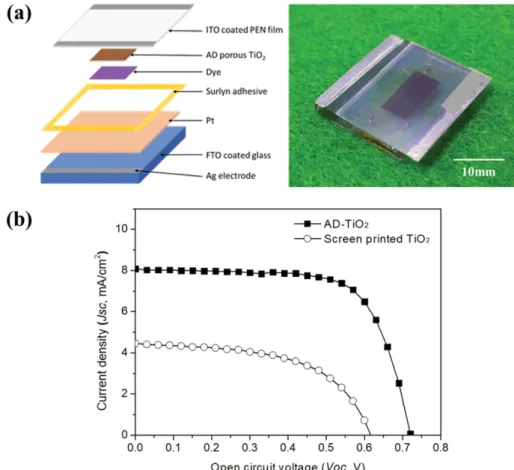
Abstract The depletion of fossil fuels and the increase in environmental awareness have led to greater interest in renewable energy. In particular, solar cells have attracted attention because they can convert an infinite amount of solar energy into electricity. Dye-sensitize solar cells (DSSCs) are low cost third generation solar cells that can be manufactured using environmentally friendly materials. However, DSSC photoelectrodes are generally produced by screen printing, which requires high temperature heat treatment, and low temperature processes that can be used to produce flexible DSSCs are limited. To overcome these temperature limitations, this study fabricated photoelectrodes using room-temperature aerosol deposition. The resulting DSSCs had an energy conversion efficiency of 4.07 %. This shows that it is possible to produce DSSCs and flexible devices using room-temperature processes.

Key words Dye-sensitized solar cell, Aerosol deposition, Photoelectrode, TiO

2

, Room temperature process

1. Introduction

The energy conversion efficiency of dye-sensitized solar cells (DSSCs) is comparable to that of amorphous- silicon solar cells. Furthermore, their simple structure and low manufacturing costs mean that they are more likely to be commercialized than other third-generation or hybrid designs. DSSCs consist of four main compo- nents: dyes with selective light absorption bands to effectively absorb visible light which comprises 44 % of the energy from the sun; photoelectrodes to transport excited electrons from the dyes; oxidated/reduced liquid electrolytes; and a transparent conductive oxide (TCO) counter electrode to allow the transmission of visible light.

TiO

2

is the most widely used photoelectrode because it is inexpensive, has a wide bandgap (3.2 eV), and good stability. The n-type photoelectrodes used in DSSCs are usually produced by screen printing with paste and ink [1-4]. Photoelectrodes manufactured using this method are heat treated at approximately 500

o

C to burn-off the binder and to develop particle-to particle connections.

However, this process is costly and limits the choice of substrate materials.

In an attempt to overcome this problem, Gutierrez-

Tauste et al. [5] and Jiang et al. [6] conducted numer- ous studies on low temperature processes using ultra- violet (UV)-irradiation and nanowires. However, they only achieved energy conversion efficiencies of less than 2 %.

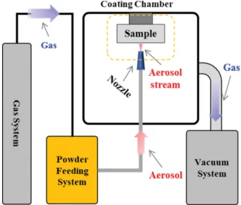
This study aims to present an improved method for manufacturing photoelectrodes using a new coating tech- nique. Here, photoelectrodes are produced using aerosol deposition on polyethylene naphthalate (PEN) films coated with transparent indium tin oxide (ITO) elec- trodes at room temperature. A DSSC fabricated using the new photoelectrode will then be compared to a tra- ditional design.

2. Experiments 2.1. Materials

TiO

2

powders, with particles 200 and 15 nm in diame- ter, were used to produce the photoelectrodes (NanoPac, Korea). Anatase phase TiO

2

was used as it is a well- known nanocrystalline particle that is stable at room tem- perature. Figure 1 shows a field electron scanning elec- tron microscopy (FE-SEM) image of the TiO

2

particles.

A PEN film (surface resistance: 15 /□) coated with a 100 nm thick layer of ITO was used as the substrate and N719 (Solaronix, Switzerland), a ruthenium com-

Corresponding author

E-mail: [email protected], [email protected]

(2)

plex that can absorb light, was used as the dye. In addi- tion, 1-methyl-3-propyl imidazolium iodide (PMII) in 3- methoxypropionitrile (MPN), a common conventional ionic liquid type electrolyte, was used as the electrolyte.

2.2. DSSC fabrication process

To make stable photoelectrodes using aerosol deposi- tion, it is important to control the moisture on the sur- face of the TiO

2

nanoparticles. Therefore, the nanoparticles were stored in a vacuum oven at 150

o

C for 24 h prior to use and 5 wt% of 15 nm particles were mixed with the 200 nm particles using a high speed mixer as required.

Figure 2 and Table 1 show a schematic of the aerosol deposition (AD) system and the main operating condi- tions used to produce the porous TiO

2

coating, respec- tively. AD is a coating technique that can produce high density and high quality ceramic layers in room-tem-

Fig. 1. FE-SEM images of used TiO

2

Particles and XRD patterns of the particles. (a) 400 nm, (b) 15 nm.

Fig. 2. Schematic of aerosol deposition system.

Table 1

Critical parameters for aerosol deposition of the TiO

2

semicon- ductor film

Parameters Value

Nozzle slit size 10 × 1.0 mm

Angle of nozzle 15

o

Working distance (Sub.-nozzle) 10 mm

Carrier gas N

2

/15 SLM

Number of scan and scan pitch2 times/0.25 mm

Scan speed 10 mm/s

perature and low-vacuum environments. Therefore, it is of interest for applications in large screen displays and plasma semiconductor equipment components where there are extreme environments. The AD system con- sisted of a coating chamber with a holder for the stream nozzle and substrate, a vacuum system, and a powder feeding system to supply the nanoparticle aerosols. Nitro- gen was used as the carrier gas for the powder and the vacuum was maintained at approximately 15 Pa as the carrier gas was injected. The TiO

2

powder was aerosol- ized by the carrier gas, transported, and sprayed at a high speed (greater than 300 m/s) through the nozzle.

The TiO

2

powder collided forcefully with the substrate and formed the TiO

2

coating. The properties of this film, such as the thickness and quality, were controlled by adjusting the angle of the nozzle, the speed, and the number of scans.

This preparation was used to apply a layer of TiO

2

(10 × 4 mm) to the ITO coated PEN film (20 × 15 mm).

This sample was immersed in 0.5 mM of N719 in ace-

tonitrile/tert-butanol solution for 24 h which adsorbed

onto the porous surface of TiO

2

. Fluoride doped tin

oxide (FTO) coated glass was used as a counter elec-

trode. This was prepared by immersing it in an aqueous

solution of 7 mM of platinum in 2-propanol. The pre-

(3)

For comparison, DSSCs were manufactured using TiO

2

photoelectrode layers of the same thickness that were fabricated by screen-printing with a binder-free paste consisting of a mixture of the same 200 and 15 nm TiO

2

particles used for the AD. The current density-voltage (I-V) curves of the DSSCs were measured using a solar simulator consisting of a xenon lamp with a light illumi- nation intensity of 100 mW/cm

2

. The results are shown in Table 2 and Fig. 3(b). The DSSC fabricated at room temperature by screen printing with the binder-free paste had a current density (J

sc

) of 4.46 mA/m

2

and an open circuit voltage (V

oc

) of 0.62 V. The fill factor (FF) and

Fig. 3. (a) Schematic and photograph of room temperature processed DSSC including AD coated porous TiO

2

as semiconductor oxide and (b) measured photovoltaic properties (I-V curve) of DSSCs.

circuit voltage of 0.72 V, fill factor of 69.41 %, and solar energy efficiency of 4.07 %, indicating overall improve- ment.

Figure 4 shows a cross-sectional SEM image of the photoelectrodes produced using a mixture containing 5 wt%

of 15 nm particles in 200 nm TiO

2

powder, or 200 nm TiO

2

powder. In general, the microstructural properties of the ceramic coating produced using AD depends on the size of the particles and the spraying speed [7-9].

For example, if the granules are too large, then the sub-

strate may be eroded or the coating may not adhere as

the collision energy of the particles is too high. In con-

(4)

trast, if the particles are smaller than several tens of nanometers, they will not have sufficient energy to form a coating because they will be scattered due to fracture- plastic deformation. Therefore, the particle size required for AD coating is approximately 1 m or less, and 200 nm TiO

2

particles are suitable for coating. However, when only 200 nm particles are used, as shown in Fig.

4(a), the coating is very dense. This is not suitable for photoelectrodes which must be porous in order to absorb the dye. Fan et al. mixed a polymer with TiO

2

to create a porous TiO

2

coating for use in DSSCs [10]. However, this required the polymer to be burnt-off at a high tem- perature of 450

o

C. Therefore, in this experiment, we have mixed 200 nm-sized TiO

2

powder, which can cre- ate a dense and hard coating film, with 15 nm-sized TiO

2

powder, which can induce a porous coating film by mit- igating collision energy, to create a coat. As described, 15 nm TiO

2

particles cannot form a coating alone because they do not have sufficient collision energy during the AD process [11]. However, if they are mixed with 200 nm particles, they can limit the collisions of the 200 nm particles or reduce their collision energy, resulting a porous coating [12]. Figure 4(b) shows a cross-sectional SEM image of a porous TiO

2

coating produced by AD without subsequent heat treatment using a 5 wt% 15 nm and 200 nm TiO

2

mixture.

These results show that the TiO

2

coating produced using AD was sufficiently porous to adsorb the dye and that there were proper connections between the TiO

2

particles without the need for heat treatment. Therefore, it effectively leads the flow of electrons.

4. Conclusion

The photoelectrodes in a DSSC must be porous to

ensure the dye is adsorbed and there must be stable con- nections between particles to guarantee the smooth flow of electrons. Therefore, it is necessary to consider the composition of the powder used to form the porous TiO

2

layer via AD. We improved the powder by mixing 5 wt% of 15 nm TiO

2

fine powder with 200 nm TiO

2

granulated powder. Then, AD was used to form a 10 m thick TiO

2

layer at room temperature and the DSSC was completed without subsequent heat treatment. To demon- strate that the AD-TiO

2

coating had a microstructure that was suitable for DSSC application, a comparison sam- ple was prepared using screen printing with binder-free paste containing the same powder without high tempera- ture heat treatment. The photovoltaic properties were then measured. The DSSC containing AD-TiO

2

per- formed significantly better than the comparison sample.

This shows that DSSCs can be manufactured at room temperature without the need for high-temperature heat treatment, which increases the potential applications of flexible DSSCs.

Acknowledgements

This work was supported by World Class 300 Project R&D Support project (www.worldclass300.or.kr) funded by the Small and Medium Business Administration (SMBA, Korea) [Project Name: Development of Plasma- resistant Surface Treatment Technology for 3D-struc- ture and Large-area Parts of Semiconductor/Display Fabrication Equipments].

References

[ 1 ] B. O’Regan and M. Gratzel, “A low-cost, high-effi- Fig. 4. Cross-sectional SEM images of AD-TiO

2

films. (a) using only 400 nm-TiO

2

powder and (b) 5 wt% 15 nm-TiO

2

mixed with

400 nm-TiO

2

. Inset shows the AD coated porous TiO

2

film on ITO-PEN film.

(5)

incorporation of TiO

2

nanoparticles into oriented TiO

2

nanotube based dye-sensitized solar cells”, J. Nanosci.

Nanotechnol. 9 (2009) 7436.

[ 5 ] D. Gutiérrez-Tauste, I. Zumeta, E. Vigil, M.A. Hernán- dezFenollosa, X. Domènech and J.A. Ayllón, “New low-temperature preparation method of the TiO

2

porous photoelectrode for dye-sensitized solar cells using UV irradiation”, J. Photochem. Photobiol. A: Chemistry 175 (2005) 165.

[ 6 ] C.Y. Jiang, X.W. Sun, K.W. Tan, G.Q. Lo, A.K.K. Kyaw and D.L. Kwong, “High-bendability flexible dye-sensi- tized solar cell with a nanoparticle-modified ZnO-nanow- ire electrode”, Appl. Phys. Lett. 92 (2008) 143101.

[10] S.Q. Fan, C.J. Li, C.X. Li, G.J. Liu, G.J. Yang and L.Z.

Zhang, “Preliminary study of performance of dye-sensi- tized solar cell of nano-TiO

2

coating deposited by vac- uum cold spraying”, Mater. Trans. 47 (2006) 1703.

[11] J. Akedo, “Room temperature impact consolidation (RTIC) of fine ceramic powder by aerosol deposition method and applications to microdevices”, J. Therm.

Spray Technol. 17 (2008) 181.

[12] H. Park, J. Kwon, I. Lee and C. Lee, “Shock-induced

plasticity and fragmentation phenomena during alumina

deposition in the vacuum kinetic spraying process”,

Scripta Mater. 100 (2015) 44.

수치

Fig. 1. FE-SEM images of used TiO 2  Particles and XRD patterns of the particles. (a) 400 nm, (b) 15 nm.
Figure  4  shows  a  cross-sectional  SEM  image  of  the photoelectrodes produced using a mixture containing 5 wt%

참조

관련 문서

5.16 Overall heat transfer coefficient and convective heat transfer coefficient of hot side according to mass flow rate and inlet temperature (High temperature condition)

That is, the expansion of material by high temperature and distortion by cooling during welding process is caused by tensile and compressive residual stresses in welding

본 실험에서는 불소이온의 흡착능력을 증대시키기 위하여 대나무 탄화물 제조를 다르게 하였다. Effect of temperature of heat treatment on the adsorption of F - by

The materials used for this research are the average temperature, maximum temperature, minimum temperature, precipitation, humidity, and sunshine duration in Honam

종류에는 Si 또는 화합물 반도체를 이용하는 무기태양전지와 나노결정산화물 입자 표면에 염료가 흡착된 염료감응형 태양전지(DSSC,Dye Sensitized Solar

▪ Local temperature of PMSM can be calculated through thermal resistance model and heat generation model, presenting the cooling performance thermal

For this reason, in this study, comparing the traditional manufacturing process and relatively high temperature of exhaust gas heat and CO2 laser

A PID control with Feedfoward Controller for Controlling Fluid Temperature in Heat Exchanger.. 지도교수