Sensor Circuit Design using Carbon Nanotube FET for Artificial Skin †
Yeon-Bo Kim
1), Kyung Ki Kim
2)Abstract This paper proposes a new sensor circuit using a 32 nm carbon nanotube FET (CNFET) technology for artificial skin. For future robotic and prosthetic applications, it is essential to develop a robust and low power artificial skin for detecting the environment through touch. Therefore, a sensor circuit for the artificial skin also has to be developed to detect the sensor signals and convert them into digital bits. The artificial skin sensor is based on a mesh of sensors consisting of a nxn matrix using CNFET, and the sensor outputs are connected to a current monitoring circuit proposed as the sensor circuit.
The proposed sensor provides pressure measurements and shape information about pressure distribution.
Key Words : Artificial skin, Carbon nanotube FET, Aritificial skin sensor, CNFET
1. Introduction†
Objects in our daily life can be picked up or moved using tough sensing. Also, the characteristics of the objects like shape and roughness is able to be detected by the sense of touch [1]. Sensing of touch is an important technique for robots of next generation, but little progress has been made, compared with other sensing techniques such as sensing of voice and sight for robots [2] since the sensing of touch is more difficulty than other sensing techniques. This is mainly because it is not easy to discover materials for the artificial skin sensor [1]. The materials for artificial skin are required not only to be low power semiconductor device but also to have flexibility characteristic to
†This research was supported by the Daegu University Research Grant, 2012.
1) Professor, Department of Electronic Engineering, Daegu University, South Korea, (e-mail: [email protected]) 2) Assistant Professor, Department of Electronic Engineering,
Daegu University, South Korea, (e-mail:[email protected]:
Corresponding author)
fit for any shape [3]. Recently, some artificial skins have been deployed in many sensor applications such as temperature sensor and light sensor.
However, the most proper application for artificial skin is combining with robots since we are in an era of robots: robots can not only move heavy objects but also do surgical operations. If the robot can feel the weight or pressure of the objects, it will be much easier for the robot to complete the tasks without breaking or dropping the objects.
Previous attempts to implement the artificial skin have depended on organic materials due to their flexibility and easy fabrication. However, the problem is that most organic materials are poor semiconductors; it means electronic devices made by the materials require high operating supply voltages.
Carbon nanotube FET (hereafter called CNFET) devices are one of the promising in-organic materials in the future. As technology scales down to 90nm and below, the bulk CMOS technology has approached the scaling limit due to the increased
short-channel effects, increased leakage power dissipation, severe process variations, high power density and so on. To overcome this scaling limit, different types of materials have been experimented, and Si-MOSFET-like CNFET devices have been evaluated as one of the promising replacements in the future nanoscale electronics. The CNFET devices have compatibility with high dielectric constant materials and a unique one-dimensional band-structure which restrains back-scattering and which makes near-ballistic operation a realistic possibility; by using this CNFET, a high-k gate oxide can be deployed for lower leakage currents while keeping the on-current drive capability (compared to Si-MOSFET); CNFET has lower short-channel effect and a higher sub-threshold slope than Si-MOSFET [4]-[7]. Therefore, the CNFET is deployed for the artificial skin sensor in this paper.
Although silicon nanowire FET (NWFET) is considered as a candidate material to implement skin sensor compared to organic material in terms of speed and flexibility due to their miniaturized dimensions, deeply scaled CNFET technology can also provide similar electrical characteristic and flexibility with NWFET. In this paper, we develop and simulate the skin sensor and the sensor interface circuit using a 32nm CNFET technology.
2. CNFET Artificial Skin Sensor 2.1 Carbon Nanotube FET
Carbon nanotube FETs employ semiconducting single-wall carbon nanotubes to assemble electronic devices, and the single walled CNFET is obtained by replacing the channel of a conventional MOSFET with carbon nanotubes (a one-dimensional conductor obtained by rolling a sheet of graphite) as shown in Fig. 1 [8][9]. The nanotubes can be either a metallic (conductor) or a semi- conducting
(semiconductor) depending on the angle (represented as a chirality integer vector (n,m)) of the atom arrangement along the nanotube. The nanotube is metallic if (n=m) or (n-m = ‘a multiple of three’), otherwise the tube is semiconducting.
(a) (b)
<Fig. 1> CNFET structure: (a) Cross sectional view, (b) Top view
As shown in Fig. 1 (a), the top gated CNFETs are fabricated on an oxidized Si-substrate that can be used as a back-gate in the CNFET. In the early 1990s, most CNFETS studied had adopted a back-gate top-contact structure [10][11], in which the nanotubes are grown on a conducting substrate covered by an insulating layer. Two metal contacts are deposited on the nanotube to serve as source and drain electrodes while the conducting substrate is the gate electrode in the three-terminal device.
However, these early CNFETs are found to have poor device characteristics such as an ambipolar transistor characteristic and gentle sub-threshold swing. In order to improve the poor device characteristics, dual-gate CNFET structures have proposed. The structures show a MOSFET-like unipolar transistor characteristic, excellent sub-threshold slopes, and a drastically improved OFF state. Each device has one or more single-wall semiconducting carbon nanotubes. The currents of the CNFET device are controlled by adjusting device parameters such as gate length (Lch), the number of nanotubes, chirality vector, and pitch between nanotubes [7][11]. As the gate voltage increases or decreases, the device is electro-
0 200m 400m 600m 800m VDS(V)
10u
0 IDS(A)
VGS 20u
30u
0 V 0.9 V NMOS CNFET
NMOS MOSFET
(a)
VGS(V) 10f
1f
Log IDS(A) VDS
100f 1p
0.1 V 0.9 V NMOS CNFET
NMOS MOSFET VDS
0.1 V 0.9 V
-0.5 -0.4 -0.2 0 0.2 0.4 0.5 10p
100p 1n 10n 100n 1u
(b)
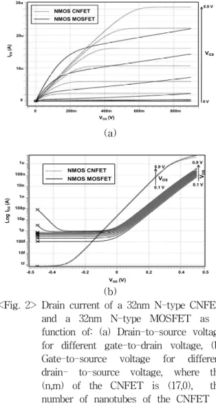
<Fig. 2> Drain current of a 32nm N-type CNFET and a 32nm N-type MOSFET as a function of: (a) Drain-to-source voltage for different gate-to-drain voltage, (b) Gate-to-source voltage for different drain- to-source voltage, where the (n,m) of the CNFET is (17,0), the number of nanotubes of the CNFET is 2, the width of the MOSFET is 64nm, the back-gate voltage is 0V, and temperature is 25°C.
statically turned on or off through the gate node.
The drain current characteristics of a 32nm N-type CNFET are presented in Fig. 2, where the characteristics are compared to those of the N-type MOSFET. IDS(drain current) of the CNFET is saturated at higher VDS (drain-to- source voltage) as VGS (gate-to-source voltage) increases as shown in Fig.2 (a), where the amount of IDS of the CNFET is greater than that of the MOSFET although the CNFET width is 6.35nm (5nm of the pitch length and 1.35nm of the diameter) and the MOSFET width is 64nm. According to the simulation results, it is possible to reduce the device size by approximately an order of magnitude if the CNFET is replaced with the MOSFET. In the sub- threshold(weak inversion) region, the characteristics of the CNFET show that IDS of the CNFET is much greater than that of MOSFET and the CNFFET almost does not have Drain-induced barrier lowering(DIBL) and Gate-induced drain leakage (GIDL) effects. As shown in the figure, CNFET on-current is higher and leakage current is lower than the MOSFET transistor. Figure 2 (b) illustrates IDS characteristics of the N-type CNFET in the weak inversion region, which implies that the CNFET would be a more practical solution even in the sub-threshold logic design requiring a smaller area than the MOSFET.
Figure 3 shows the back-gate voltage (VBG) impact on the drain current (IDS) of a 32nm NMOS CNFET; VBG increases IDS approximately by 30%
depending on the top-gate voltage VGS). Especially, a small amount of drain current can be generated by VBG at zero gate voltage.
2.2 Arttificial Skin Sensor
The skin sensor can sense four kinds of different sensing mechanism such as static pressure, touch, vibration and stretch as shown in Fig. 4: each sensing mechanism has different frequency. The skin sensor circuit is shown in Fig. 5. The skin
sensor circuit in Fig. 5 is constructed with n columns and n rows using P-type CNFETs. The gate of each P-type transistor is connected to the row selection block, and the source of each P-type transistor is connected to the column selection block. The drain of each P-type CNFET transistor is connected to pressure-sensitive rubber (PSR).
The characteristic of the PSR is that when the material is exposed to pressure, the conductance will be changed due to the shortened tunneling path between the conductive carbon nano-particles
10u
0 IDS(A)
20u 30u
W/ Back gate biasing W/o Back gate biasing
VGS(V)
-0.5 0 0.5 1.0 VBG
0.1 V 0.9 V
VBG=0 40u
3.0n
0 1.0n 2.0n
-0.5 0 0.2 VBG
0.1 V 0.9 V
VBG=0
VGS (V) IDS(A)
<Fig. 3> Drain current of a 32nm N-type CNFET as a function of Gate-to-source voltage for different back-gate voltage, where the (n,m) of the CNFET is (17,0), the number of nanotubes of the CNFET is 2, the width of the MOSFET is 64nm, and temperature is 25°C.
<Fig. 4> Different skin sensing Mechanism
<Fig. 5> Skin sensor circuit structure
embedded in the rubber. Therefore, in circuit
simulations, the PSR is modeled as a resistor with variable resistance value. While the skin sensor is exposed to pressure, the P-type CNFET transistor is turned on, and then resistance value of each PSR is decided depending on the pressure. When the skin sensor is touched, the row-selection and column-selection blocks will precisely select P-type CNFET transistors on the location where the resistance value of PSR is changed, then the selected transistors will be turned on, and current will flow through the PSR. By differentiating the current value from each pixel, the location of the pressure is detected in a main control system.
3. Sensing Circuit for the artificial skin Fig. 6 shows a proposed current monitoring circuit used as a sensor interface circuit for each cell. When the cell is pressed, different current flows through PSR depending on the pressure. The M1 devices in Fig.6 are operated as current mirrors for generating the reference currents depending on the Wp size.
The NMOS devices with Wn size are deployed to generate currents depending on the PSR voltage. If higher pressure is presented at a cell, more current flows through the PSR, and the current value at M1 increses. The increased current generates current flowing through each NMOS connected by M1. Each current source value is compared with PSR current IPSR. Each inverter generates logic 1 if the current value of the current source is smaller than that of IPSR, and it generate logic 0 if he current value of the current source is greater than that of IPSR. By using this circuit scheme, different pressure at the pixel is represented by combination of the output logic values. The area of one pixel and its current monitoring circuit is very small for flexible skin sensor application.
4. Simulation Results
The skin sensor circuit shown in Fig. 3 with n=12 is simulated using CNFET using 32nm technology. The current value at each transistor is measured when the pressure presents. Then, the current value at each pixel (transistor) is imported to MATLAB which displays the image representing the pressure point of the skin sensor. As shown in Table 1, the huge current difference is generated by the pressure value of the skin sensor.
<Fig. 6> Current monitoring circuit (digital- izing) for a cell
<Table 1> Average Current Value for Pressed Pixel and Unpressed Pixel (VDD=0.9V)
CNFET
Pixels Pressed unpressed Average Current (A) 1.2E-5 1.8E-16
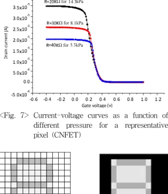
As shown in Fig. 7, when a pixel on a skin sensor is pressed, the P-type CNFET is turned on, and the amount of current flowing through PSR is determined according to the pressure value. The higher pressure is applied, the higher current at each pixel flows.
Fig. 8 (a) assumes that the skin sensor circuit is pressed with number ‘8’ shape for the pressure distribution. The PSR demonstrates different resistance according to the pressure value, and different drain to source current is observed at each pixel. MATLAB codes are programmed to take all the currents at each pixel as input. All the current values are quantized and the quantized values are
mapped to 0 to 255 gray scale. Fig. 8 (b) shows the MATLAB simulation results precisely indicating the location of the pressure, and the gray is the level of the pressure.
<Fig. 7> Current-voltage curves as a function of different pressure for a representative pixel (CNFET)
(a) (b )
<Fig. 8> Simulation for skin sensor circuit (a) pressure geometry for skin sensor circuit; (b) output image from MATLAB according to skin sensor pressure location
However, in real circuit, leakage current of the device cannot be avoided. Some pixels which do not suffer pressure can be selected by row selection at the gate node of each transistor or column-selection block at the source node of each transistor due to leakage current flowing through the PSR, which results in the gray area around the pressure location.
The proposed CNFET skin sensor circuit for different supply voltages has been simulated to show the performance in terms of power and delay.
The power consumption has been measured for the dynamic power of the circuit while the delay has been measured for the PSR voltage charging time.
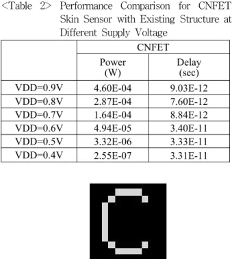
<Table 2> Performance Comparison for CNFET Skin Sensor with Existing Structure at Different Supply Voltage
CNFET Power
(W)
Delay (sec) VDD=0.9V 4.60E-04 9.03E-12 VDD=0.8V 2.87E-04 7.60E-12 VDD=0.7V 1.64E-04 8.84E-12 VDD=0.6V 4.94E-05 3.40E-11 VDD=0.5V 3.32E-06 3.33E-11 VDD=0.4V 2.55E-07 3.31E-11
<Fig. 9> Matlab simulation result using proposed skin sensor circuit using CNFET
(a) (b)
<Fig. 10> Matlab simulation results for (a) vibration sensing and (b) stretch sensing using proposed skin sensor circuit in CNFET
The CNFET skin sensor circuit is both implemented in 32nm technology with the same channel length (32nm) and transistor width (64nm).
As shown in Table 2, at each supply voltage level, CNFET demonstrates lower power consumption and faster speed because CNFET skin sensor operates at 0.4V.
Although the CNFET operates at low voltage, CNFET skin sensor still shows better speed and power performance. The simulation results in Table 2 show that CNFET skin sensor can be applied in the sub-threshold region to achieve ultra-low power consumption while keeping high speed.
Fig. 9 shows the Matlab simulation results using proposed skin sensor circuit. As shown in Fig. 9, the sensitivity of the skin sensor detecting the pressure is improved compared with the results shown in Fig. 8 (b) due to the leakage current reduction.
Fig. 10 demonstrates the vibration sensing and stretch sensing using the skin sensor. For Fig. 10 (a), assuming the vibration source is at point P, the current status of the skin sensor has been captured at a certain time during the vibration. As it is shown in Fig. 10 (a), the highest current presents at the vibration point P, which means P suffers from the highest pressure. The vibration force reduces from the center to the boarder side of the skin sensor. Therefore, pixels located far away from the center P suffer less pressure, hence less currend has been generated. Fig. 10 (b) shows that the skin sensor is under stretch. The stretch forces are applied on the left and right boarders. Therefore, these two boarders suffer the highest pressure while less pressure is observed toward the center of the skin sensor.
5. Conclusions
In this paper, we propose a sensor circuit for the skin sensor using CNFET at 32nm technology. The skin sensor is considered as a critical component for the robot sensing application. We have simulated and analyzed the performance for CNFET skin
sensor. A MATLAB function has been implemented to demonstrate the output image according to the skin sensor’s pressure location and the amount of the pressure. In addition, we show that the CNFET circuit can reduce power consumption while keeping high speed.
References
[1] Takei K, Takahashi T, Ho JC, Ko H, Gillies AG, Leu PW, Fearing RS, Javey A., "Nanowire active-matrix circuitry for low-voltage macroscale artificial skin," Nature Mater. 2010 Oct pp. 821-826.
[2] Sergio, M. Manaresi, N. Campi, F. Canegallo, R.
Tartagni, M. Guerrieri, R., "A dynamically reconfigurable monolithic CMOS pressure sensor for smart fabric," Solid-State Circuits, IEEE Journal, Volume: 38, pp. 966 - 975.
[3] Someya, T., "Integration of organic field-effect transistors and rubbery pressure sensors for artificial skin applications," Electron Devices Meeting, 2003., pp. 8.4.1 - 8.4.4.
[4] A. Rahman, J. Guo, S. Datta, M.S. Lundstrom,
“Theory of ballistic nanotransistors,” IEEE Trans. Electron Devices, vol. 50, no. 10, pp.
1853- 1864, Sept. 2003
[5] A. Akturk, G. Pennington, N. Goldsman, “A.
Wickenden, Electron Transport and Velocity Oscillations in a Carbon Nanotube,” IEEE Trans.
Nanotechnol., Volume 6, Issue 4, pp 469 – 474, July 2007.
[6] Haiqing and Ken Choi, “Novel ternary logic design based on CNFET, ” International SoC Design Conference, 2010, pp. 115-118.
[7] Jie Deng, H.-S.P. Wong, “A Compact SPICE Model for Carbon-Nanotube Field-Effect Transistors Including Nonidealities and Its Application?Part I: Model of the Intrinsic Channel Region,” IEEE Trans. Electron Device, vol. 54, no. 12, pp. 3186 - 3194, Dec. 2007
[8] H. Hashempour, F. Lombardi, “Device model for ballistic CNFETs using the first conducting band,” IEEE Design and Test of Computer, vol.
25, issue 2, pp 178-186, March-April 2008.
[9] Y. Lin, J. Appenzeller, J. Knoch, P. Avouris,
“High-performance carbon nanotube field-effect transistor with tunable polarities,” IEEE Trans.
Nanotechnol., Vol 4, Issue 5, pp 481 - 489, Sept.
2005.
[10] P. L. McEuen, M. S. Fuhrer, and H. Park,
“Single-walled carbon nanotube electronics,”
IEEE Trans. Nanotechnology, vol. 1, no. 1, pp.
78-85, Mar. 2002.
[11] P. Avouris, J. Appenzeller, R. Martel, and S. J.
Wind, “Carbon nanotube electronics,” Proc. of IEEE, vol. 91, no. 11, pp. 1772-1784, Nov. 2003.
김 연 보 (Yeon-Bo Kim)
∙정회원
∙1979년 2월 영남대 전자공학과 공학사
∙1981년 2월 영남대 전자공학과 공학석사
∙1996년 2월 영남대 전자공학과 공학박사
∙1983년 3월 ∼ 현재 대구대학교 정보통신대학 전자 전기공학부 교수
∙관심분야 : 전자세라믹 및 초음파공학
김 경 기 (Kyung Ki Kim)
∙정회원
∙1995년 8월 영남대 전자공학과 공학사
∙1997년 8월 영남대 전자공학과 공학석사
∙2008년 1월 (미) Northeastern University 전기전자 공학과 공학박사
∙2008년 2월 ∼ 2009년 1월 (미) SUN Microsystems 연구원 (Technical Staff)
∙2009년 1월 ∼ 2010년 2월 (미) Illinois Institute of Technology 연구원
∙2010년 3월 ∼ 현재 대구대학교 정보통신대학 전자 전기공학부 조교수
∙관심분야 : SoC 설계, Microprocessor, High performance and low power design methodo- logy, Nanotechnology.
논 문 접 수 일 1 차 수 정 완 료 일 2 차 수 정 완 료 일 게 재 확 정 일 : : : :
2014년 01월 13일 2014년 03월 04일 2014년 04월 11일 2014년 05월 09일