Nomenclature
a-Si:H : Hydrogenated amorphous silicon
p-nc-SiC:H : P-type hydrogenated nanocrystalline silicon carbide
i-a-Si:H : Intrinsic hydrogenated amorphous silicon V
OC
: Open-circuit voltage, V
J
SC
: Short-circuit current density, mA/cm
2
FF : Fill factor
EQE : External quantum efficiency
PECVD : Plasma-enhanced chemical vapor deposition BIPV : Building-Integrated Photovoltaics
1. 서 론
급격한 산업화 및 도시 확장으로 인하여 도시 내 건물들의 과 도한 에너지 소비는 온실가스 배출 등의 환경오염에 큰 영향을 미치고 있다. IPCC (Intergovernmental Panel on Climate Change) 제 5차 보고서에 따르면, 온실가스 배출은 산업부문이 31%, 건 물부문이 19%로 건물 배출량이 두 번째로 높으며 에너지 소비
DOI:https://doi.org/10.21218/CPR.2019.7.4.097 eISSN 2508-125X
광흡수층 두께에 따른 투광형 비정질 실리콘 박막 태양전지의
양면발전 성능특성
서영훈1,2)ㆍ이아름1)ㆍ신민정1)ㆍ조아라1)ㆍ안승규1)ㆍ박주형1)ㆍ유진수1)ㆍ최보훈2)*ㆍ조준식1)*
1)태양광연구실, 한국에너지기술연구원, 대전, 34129
2)신소재물리학과, 동아대학교, 부산, 49315
Impact of Absorber Thickness on Bifacial Performance Characteristics of Semitransparent Amorphous
Silicon Thin-Film Solar Cells
Yeong Hun Seo1,2) ․ Ahruem Lee1) ․ Ara Cho1) ․ Min Jeong Shin1) ․ Seungkyu Ahn1) ․ Joo Hyung Park1) ․
Jinsu Yoo1) ․ Bo-Hun Choi2)* ․ Jun-Sik Cho1)*
1)
Photovoltaics Laboratory, Korea Institute of Energy Research, Daejeon 34129, Korea
2)
Department of Materials Physics, Dong-A University, Busan 49315, Korea
Received September 25, 2019; Revised December 5, 2019; Accepted December 8, 2019
ABSTRACT: Bifacial and semitransparent hydrogenated amorphous silicon (a-Si:H) thin-film solar cells in p-i-n configuration were prepared with front and rear transparent conducting oxide (TCO) electrodes using plasma-enhanced chemical vapor deposition method.
Fluorine-doped tin oxide and tin-doped indium oxide films were used as front and rear TCO contacts, respectively. Film thickness of intrinsic a-Si:H absorber layers were controlled from 150 nm to 450 nm by changing deposition time. The dependence of performance characteristics of solar cells on the front and rear illumination direction were investigated. For front illumination, gradual increase in the short-circuit current density (J
SC
) from 10.59 mA/cm
2 to 14.19 mA/cm
2 was obtained, whereas slight decreases from 0.83 V to 0.81 V for the open-circuit voltage (V
OC
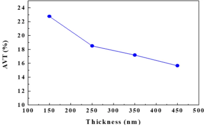
) and from 68.43% to 65.75% for fill factor (FF) were observed. The average optical transmittance in the wavelength region of 380 ~ 780 nm of the solar cells decreased gradually from 22.76% to 15.67% as the absorber thickness was changed from 150 nm to 450 nm. In case of the solar cells under rear illumination condition, the J
SC
increased from 10.81 to 12.64 mA/cm
2 and the FF deceased from 66.63% to 61.85%, while the V
OC
values were maintained at 0.80 V with increasing the absorber thickness from 150 nm to 450 nm. By optimizing the deposition parameters, a high-quality bifacial and semitransparent a-Si:H solar cell with 350 nm-thick i-a-Si:H absorber layer exhibited the conversion efficiencies of 7.69% for front illumination and 6.40% for rear illumination, and average visible optical transmittance of 17.20%.
Key words: Bifacial, Semitransparent, Absorber, Amorphous silicon, Conversion efficiency, Optical transmittance
ⓒ 2019 by Korea Photovoltaic Society
This is an Open Access article distributed under the terms of the Creative Commons Attribution Non-Commercial License (http://creativecommons.org/licenses/by-nc/3.0)
which permits unrestricted non-commercial use, distribution, and reproduction in any medium, provided the original work is properly cited.
97