• 검색 결과가 없습니다.

Design and Implementation of a Face Recognition System-on-a-Chip for Wearable/Mobile Applications

N/A
N/A
Protected

Academic year: 2021

Share "Design and Implementation of a Face Recognition System-on-a-Chip for Wearable/Mobile Applications"

Copied!
9
0
0

로드 중.... (전체 텍스트 보기)

전체 글

(1)

ABSTRACT

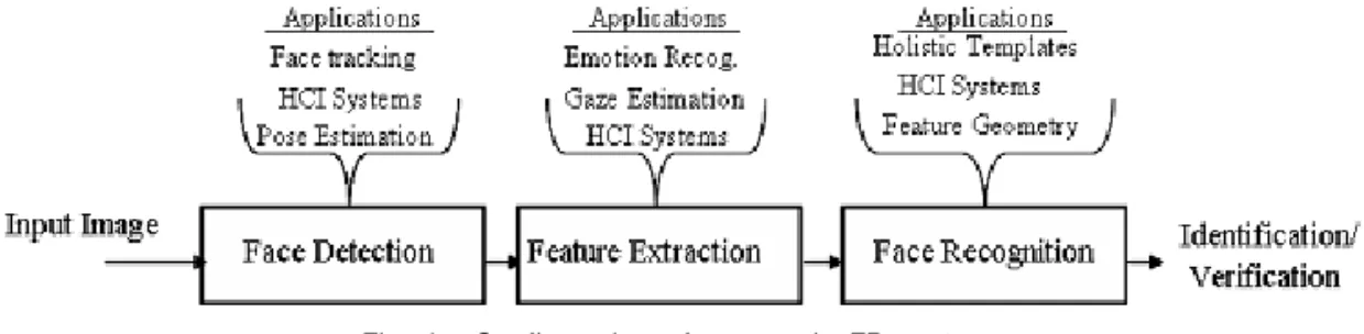
This paper describes the design and implementation of a System-on-a-Chip (SoC) for face recognition to use in wearable/mobile products. The design flow starts from the system specification to implementation process on silicon. The entire process is carried out using a FPGA-based prototyping platform environment for design and verification of the target SoC. To ensure that the implemented face recognition SoC satisfies the required performances metrics, time analysis and recognition tests were performed.

The motivation behind the work is a single chip implementation of face recognition system for target applications.

Key words: Face Recognition, Wearable, FPGA, SoC

※ Corresponding Author : Bongkyu Lee, Address: (690- 756) Dept. of Computers & Statistics, Jeju National University, Jeju-daehakro 66, Jeju City, Jeju-Do, TEL : +82-64-754-3593, FAX : +82-64-725-2579, E-mail : bklee

@jejunu.ac.kr

Receipt date : Jan. 7, 2015, Revision date : Jan 21, 2015

Approval date : Feb. 13, 2015

††

Dept. of computer science and Statistics, Cheju National University

※ This research was supported by the 2014 scientific promotion program funded by Jeju National University

1. INTRODUCTION

Face Recognition (FR) is an integral part of wearable/mobile systems like memory aids or con- text awareness systems. Thus, developers will in- tegrate FR system with clothing, accessories and mobile phones. For instance, FR systems em- bedded into eyeglasses can help us remember the name of the person we are looking at by recogniz- ing their face from a stored database of images and

“whispering” the person’s name into our ear [1].

Although many FR techniques have been pro- posed thus far [2], FR system for wearable/mobile applications still remains to be a challenging prob- lem. Wearable/mobile computing devices have constraints in their processing capabilities because of cost and power consumption, while generic FR systems (Fig. 1) require a large amount of re- sources for sufficient accuracy [2]. Also, since wearable/mobile devices should be as light and as

small as possible, an embedded FR system or- ganized on a Printed Circuit Board (PCB) are in- appropriate for wearable/mobile applications.

A System-on-a-Chip design methodology can be used to integrate entire components of a target system into single chip so that it can be applied to one-chip implementation of FR for wearable/

mobile applications with compact size and weight.

In this paper, we propose a new FR SoC archi- tecture for wearable/mobile computing and appli- cations. The implementation steps are as follow.

First, we designed and implemented the prototyp-

ing emulation platform based on a Field Program-

mable Gate Array (FPGA). This emulation plat-

form was used for testing and debugging the target

SoC architecture in the register transfer level. We

performed a comprehensive analysis of the compu-

tational characteristics of a FR algorithm on the

emulation platform. Then, we selected some soft-

ware modules that should be implemented into

(2)

Fig. 1. Configuration of a generic FR system.

hardware because of their intensive computing requirements. We designed hardware logics for se- lected software modules and mapped them into the FPGA. Other modules of the FR algorithm were stored into the memory that will be implemented into a final SoC. We evaluated the performances of the implemented FR SoC in the register transfer level using the emulation platform and observed that the implemented FR SoC can be used for vari- ous wearable/mobile applications.

2. RELATED WORKS

Embedded FR systems can be mainly divided into three categories; fully software implementa- tion [3-5], fully hardware implementation [6,7] and SoC design method [8-10]. A fully software im- plementation is more flexible, easier in developing and debugging. However, this method usually re- quires higher hardware capabilities such as a pow- erful processor and a large amount of memory.

Therefore, this method is not suitable for mo- bile/wearable applications which have only re- stricted hardware resources.

A fully hardware implementation is charac- terized by its high speed, concurrency and lower power consumption. In [6] and [7], the face de- tection stage and feature extraction stage were im- plemented using this method. However it is diffi- cult to design and debug compared to other methods. Also, pure hardware implementations of the feature extraction and recognition stages are not effective in terms of cost and implementation complexity compared to other methods [3,9,10].

The SoC method is carried out by analyzing the timing of the different portions of the algorithm and implementing the time-extensive parts as hard- ware. This method gives the capability of integrat- ing different functions into a chip. In [9], the face detection stage was implemented onto a reconfig- urable hardware according to the SoC method.

However, the implementation only aimed at face detection so that it cannot be used for FR applica- tions directly. In [8] and [10], they designed a set of fixed-point custom hardware instructions into a FPGA for time consuming functions, such as square root and arc tangent. Since the custom hardware instruction-based optimization of the FR algorithm reduced the execution time under an em- bedded environment, these approaches have many advantages in terms of flexibility and efficiency.

However the former implementation [8] [10] cannot be directly applied to real FR applications, since their approaches were not considered ‘real-life’ en- vironments [3].

3. THE FR SoC EMULATION FRAMEWORK

3.1 The prototyping platform and the operating software

To design and verification of SoC, FPGA-based emulation platform has become popular in co-ver- ification and rapid prototyping [11]. Mapping the entire design of the target SoC into an FPGA gives an accurate and fast representation.

For the prototyping platform based on a FPGA,

the basic components, - including CPU, several

system buses and associated interconnection blocks,

(3)

Fig. 2. The prototyping emulation platform.

Fig. 3. The monitor program.

ors was 30MHZ. For acquisition of images, a MICRON MT9V112 image sensor [13] was con- nected to the emulation platform using an I

2

C bus which was implemented in the FPGA.

The emulation platform has the SDRAM-based memory (128 Mbytes, SAMSUNG 16bits × 2) and the Flash-based storage (8 Mbytes, INTEL STRATA 16bits × 2). SDRAM-based memory unit is used for storing images captured by the image sensor, while Flash-based storage is used for storing co- des (program) and data. Fig. 2 shows the im- plemented emulation platform with compact size of 112 × 129 mm.

We designed small interactive bootstrap pro- gram for operating the emulation platform. Fig. 3 shows the flow of the bootstrap program. First, it initializes the hardware components, such as I/O interfaces, memory, serial port units and timer/in- terrupt units. After hardware initialization, the pro- gram waits for the command produced from ex- ternal buttons. The emulation platform has 4 but- ton inputs (commands); enrollment, recognition, debugging and reset. The program analyzes re- ceived commands, and executes the appropriate routine for that command. By using this program, the overhead of operational software was greatly reduced.

2.2 The FR algorithm

Fig. 4 shows the FR algorithm that was used for design and implementation of the FR SoC. It was executed and analyzed on the emulation platform. The algorithm consisted of three stages;

the face detection stage, the feature extraction stage and the recognition stage. The face detector consisted of two multi-layer perceptrons, the fast search network and the fine search network. In [14], they showed that neural networks can effec- tively used to face detection task. The structure of each network was three-layer (input/hidden/

output) and fully connected perceptron.

The fast search network searches face candi-

dates (30 × 30 sized region) in input images, while

the fine search network is for searching actual face

regions (size of 20 × 20 pixels) among face candi-

dates obtained by the fast search network. Input

nodes of the fast search network receive original

intensity and histogram equalized intensity of each

pixel so that the number of input nodes is 2N,

where N is the dimension of input vectors. Input

nodes of fine search network use histogram equal-

ized intensity and lightening corrected intensity of

each pixel so that the number of input nodes is also

(4)

Fig.4. Block diagram of the FR algorithm.

2N. Position relative feature vectors [15] of nose, mouth and lips of each detected face were ex- tracted for recognition. Covariance distances be- tween an input image and enrolled DB entries were measured for recognition. The algorithm was im- plemented by building a C program. The original algorithm had showed 93.4% of the face detection rate and 89.0% of the recognition rate with FERET [16] face database.

Since the FR algorithm should be executed on the emulation platform, we have employed many engineering solutions into the original FR codes.

A floating point computation was converted into an integer computation by normalizing the oper- ands into an integer under certain operator. In some cases, multiplication was converted into addition.

Also some intrinsic functions, such as cosine and hyper tangent, were converted into table lookups.

After modifications, final C codes were translated into an executable codes for LEON 2 using BCC- bare C cross compiler [11].

2.3 Timing analysis and partitioning

Next step in the design process was to perform timing analysis for the different software functions of the algorithm on the emulation platform. We an- alyzed the computational requirements of the modified FR codes under a face database which has

200 images of 20 persons. 320 × 240 sized images were captured in the environment of large var- iances in illumination and poses. Three images of each person were used for enrolling so that the ex- perimental DB contained 60 images. Calculating the elapsed time taken by each function was used to select time-consuming modules of the algorithm.

We did this analysis by inserting software time- stamps between the functions.

After performing this step, we found out that the face detection phase took 89% (89 seconds) of the entire processing time (100 seconds). The face de- tection phase consisted of four modules (as shown in Fig. 4), image pyramid generation, histogram equalization and lightening correction and two neural-based detectors. Among them, two neural network based face detectors consumed 76% (68 seconds) of the entire processing times for face de- tection phase. The image pyramid generation rou- tine took 17% (15 seconds) of the entire processing times for face detection phase. Histogram equal- ization and lightening correction required 7% (6 seconds) of the total elapsed time (100 seconds).

Generally, a neural network requires M × N × K

times of ‘Sum Of Products’ (SOP) [15], where M

is the number of output nodes, N is the number

of hidden nodes and K is the number of input

nodes. This intensive computation requires power-

(5)

as the above two modules, they also required extra times for their own tasks. As a conclusion, these four modules should be implemented as hardware logics in the SoC.

4. SoC IMPLEMENTATION

In this section, we have focused on the design and implementation details of two hardware blocks for face detection phase

2.1 The pyramid reduction block

Fig. 5-a shows the architecture of the hardware block for production of a sequence of reduced im- ages of an original image, called image pyramid [14]. A generated image pyramid is used for finding faces that are larger than the size of predefined processing window, which are 30 × 30 (in the case of the fast search) or 20 × 20 (in the case of fine search). Since continuous reductions with respect to the original image can be achieved by smoothing the image with a smoothing kernel and the scale parameter, the block used the scale factor 1.25 and 3-tap Gaussian filter. The block receives a 320x 240 sized image stored in SRAM-based memory and constructs an image pyramid using internal working memory A and B as shown in Fig. 5-a.

The generated image pyramid is stored into the SRAM-based memory for the FR coprocessor block, the face detector. Fig. 5-b shows the control path of the block.

2.2 The FR coprocessor block

Fig. 6-a. shows the block diagram of FR co- processor block, the face detector. It consists of two hardware logic blocks, the preprocessing block

fast search phase.

The neural network logic block receives its in- puts from preprocessing sub-block and computes the output values of hidden and output nodes. First, all output values of hidden nodes are calculated by SOP between input nodes and input-hidden weights. Then, the output value is calculated by SOP between outputs of hidden nodes and hid- den-output weights. Weight values were stored as 12 bits precision in the internal ROM. The activa- tion function (hyper-tangent) for each node was computed by table-lookup method, which the table was stored in the ROM with 8 bits precision. Fig.

6-b shows the control path of the co-processor for performing the task.

The preprocessing block and the neural network computation block are operated simultaneously us- ing two buffers ‘A’ and ‘B’. The preprocessing hardware reads the image from buffer ‘A’ and starts its tasks. During the processing with an im- age from the buffer ‘A’, another 30x30 image is stored in the buffer ‘B’. When the preprocessing block completes tasks with an image in buffer ‘A’, it transfers the result image to neural network block and read an image in buffer ‘B’ for the next process. The neural network block starts its task simultaneously when the preprocessing block starts with an image in the buffer ‘B’. Fig. 7 illus- trates the pipeline processing between two hard- ware blocks.

5. IMPLEMENTATION AND EVALUATION

All hardware modules were fully synthesized by

VHDL model and mapped into FPGA. Fig. 8 shows

the chip level design, which has processors, system

(6)

(a) Block diagram of pyramid architecture

(b) The control path of the block Fig. 5. The pyramid construction block.

buses and two FR related blocks at the register transfer level. It works as the prototyping chip of the target FR SoC.

The SoC performs full FR phases itself without additional hardware or software. When enroll or recognition button is pressed, a FR task will be performed as following steps. The camera captures a facial image and transmits it to the SRAM-based memory. Then, face detection phase is performed by two hardware logics, pyramid reduction and face recognition co-processor. Detected face re- gions are stored into SRAM-based memory for next phases. After the face detection stage, the feature extraction and the recognition phases are performed using software modules stored in the

Flash memory. Recognition results are finally dis- played on the LED.

For the evaluation of the implemented system, we performed recognition experiments using seven images of each person with our experimental DB (60 images for 20 persons). Recognition rates, face detection rates and required times were compared to the fully software implementation. Table 1 shows detection rates, recognition rates and re- quired tines of two methods.

The implemented SoC is lower detection and

recognitions rates compared to the fully software

implementation method. This is because of pre-

cision parameters of the implemented Soc such as

integers, floats and others. However, the im-

(7)

(a) Block diagram of the co-processor

(b) The control path of the neural network computation sub-block Fig. 6. Face detection coprocessor.

Table 1. Evaluation results of two methods Parameters Our SoC Software_

version Face Detection rate (%) 93 96

Recognition rate (%) 89 93

Required Time for

processing (Sec) 12 100

plemented SoC only required 12 seconds, since the face detection time can be reduced to less than one second by the hardware implementation. Although feature extraction and recognition phases required 7.0 and 4.0 seconds respectively, we verified that reduction of times for feature extraction and recog- nition can be obtained by higher operational clock

speed of the processors. Thus, the implemented FR SoC can be effectively used for various real-time applications.

6. DISCUSSION AND CONCLUSIONS

In this paper, we designed and implemented a new FR SoC architecture for wearable/mobile applications. The FR SoC was tested and verified in the register transfer level architecture using FPGA-based emulation platform. All components of hardware and software were directly integrated into the implemented SoC. This FR SoC can be ef- fectively used to give intelligence to wearable/

mobile systems. We are going on the chip fabric

(8)

Fig. 7. The pipeline scheme between sub-blocks.

Fig. 8. The block diagram of architecture level design.

process for our FR SoC. Also, we hope to improve our FR algorithm for achieving better recognition rates and speed.

REFERENCE

[ 1 ] Pentland and T. Choudhury, “Face Recognition for Smart Environments,” IEEE Computer, Vol. 33, No. 2, pp. 50-55, 2000.

[ 2 ] W. Zhao, R. Chellappa, P.J. Philips, and A.

Rosenfeld, “Face Recognition: A Literature Survey,” ACM Computing Surveys, Vol. 35, No. 4, pp. 399-458, 2003.

[ 3 ] N. Arshad, K. Moon, and J. Kim, “A Secure Face Cryptography for Identity Document Based on Distance Measures,” J ournal of Korea Multimedia Society, Vol. 16, No. 10, pp.

1156-1162, 2013.

[ 4 ] A. Colmenarez, B. Frey, and T.B. Huang,

“Embedded Face and Facial Expression Recognition,” Proceeding of the IEEE Con-

ference on Computer Vision and Pattern Recognition, pp. 633-637, 1999.

[ 5 ] J. Yang, X. Chen, and W. Kunz, “A PDA- based Face Recognition System,” Proceeding of WACV 2002, pp. 19-23, 2002.

[ 6 ] S. Kwon, “Face Detection Algorithm Using Color Distribution Matching,” Journal of Korea Multimedia Society, Vol. 16, No. 8, pp.

927-933, 2013.

[ 7 ] D. Kim, I. Jeon, S. Lee, P. Rhee, and D. Chung,

“Embedded Face Recognition based on Fast Genetic Algorithm for Intelligent Digital Photography,” IEEE Transactions on Consu- mer Electronics, Vol. 52, No. 3, pp. 726-734, 2006.

[ 8 ] S. Song and S. Park, “Design of a Wide Tuning Range DCO for Mobile-TV Applica- tions,” Journal of Korea Multimedia Society, Vol. 14, No. 5, pp. 614-621, 2011.

[ 9 ] R. McCready, “Real-Time Face Detection on

a Configurable Hardware System,” Proceed`ing

(9)

Test in Europe, pp. 1-6, 2006.

[11] J. Lim, S. Park, and J. Park, “Design to Chip with Multi-Access Memory System an Parallel Processor for 16 Processing Elements of Image Processing Purpose,” J ournal of Korea Multimedia Society, Vol. 14, No. 11, pp.

1401-1408, 2013.

[12] LEON2 Processor User’s Manual, Gaisler Research, 2003.

[13] MT9V112 Manual, Micron Technology Inc., 2003

[14] H. Rowley, S. Balujua, and T. Kanade,

“Neural Network-based Face Detection,”

IEEE Transactions on PAMI, Vol. 20, No. 1, pp. 23-28, 1998.

[16] P.J. Phillips, H. Moon, P.J. Rauss, and S. Rizvi,

"The FERET Evaluation Methodology for Face Recognition Algorithms," IEEE Tran- sactions on PAMI, Vol. 22, No. 10, pp. 719- 721. 2000.

Bongkyu Lee

He received the Ph.D degree

from the Department of com-

puter engineering, Seoul Natio-

nal University in 1995. Since

1996, he has been a professor at

the Jeju national university. His

interesting research fields are in

Neural Networks, image processing and Augmented

Reality.

수치

Fig. 1.  Configuration of a generic FR system.
Fig. 2. The prototyping emulation platform.
Table 1. Evaluation results of two methods Parameters Our SoC Software_
Fig. 8. The block diagram of architecture level design.

참조

관련 문서