http://dx.doi.org/10.3938/NPSM.68.834
Fabrication of Microholes in Silicon Wafers by Using Wet-Chemical Etching
Ha Young Lee · Ji-Yeon Noh · Min Sub Kwak · Kyung-Won Lim
· Hyung Soo Ahn · Ji-Hoon Ahn · Sam Nyung Yi
∗Department of Electronic Materials Engineering, Korea Maritime and Ocean University, Busan 49112, Korea
Jungho Ryu
†School of Materials Science and Engineering, Yeungnam University, Gyeongsan 38541, Korea (Received 18 April 2018 : revised 16 July 2018 : accepted 17 July 2018)
The presence of microholes gives materials unique physical properties through their effect on both light and matter. In particular, they can be widely used to increase the efficiency of devices such as light-emitting diodes (LEDs), organic LEDs (OLEDs), solar cells, and sensors. They also have various applications such as aiding plasmon formation on a metal surface. This work reports the quick and inexpensive formation of large amounts of microholes through wet-chemical etching. A Si(100) substrate was etched with KOH solution; the resulting holes depended on the temperature and etching duration. Reacting Si and KOH solution (20%) at 70, 80 and 90 ◦C resulted in microholes. Field-emission scanning electron microscopy (FE-SEM) was used to investigate the mechanism and the rate of etching with respect to temperature and etching duration. The completed microholes can be finely adjusted through the deposition of a metal such as Au, Pt, Ag or Cu to give them properties suitable for various uses.
PACS numbers: 81.65.Cf, 52.77.Bn, 93.85.Fg Keywords: Si, Wet-chemical etching, Microholes
I. INTRODUCTION
Microholes exploit the coupled interactions of light and matter to achieve unique properties [1–6]. In par- ticular, metallic microhole structures exhibit strong res- onances when illuminated with ultraviolet, visible, or near-infrared light in the vicinity of their surface plas- mon polariton frequencies [7–9]. The discovery of en- hanced optical transmission through subwavelength hole arrays has attracted considerable interest in optical phe- nomena and their possible applications such as increas- ing the efficiency of light-emitting diodes (LEDs), or- ganic LEDs (OLEDs), solar cells, and sensors [10–16].
However, techniques employed to fabricate microholes (e.g., focused ion beam [17,18], soft lithography [19,20], nanoimprint lithography [21,22], X-ray lithography [23,
∗E-mail: [email protected]
†E-mail: [email protected]
24], and reactive ion etching [25,26]) are time consuming and require expensive equipment and professional staff.
Therefore, we developed a method to create microholes by wet-chemical etching a Si substrate.
Silicon is widely used in many fields because it is cheap and strong, among other advantages. It is compatible with wet-chemical etching, which is widely used to fabri- cate various structures, from simple cavities to complex patterns. This technique’s major advantages include low cost and ease of use, and thus it can help minimize fab- rication costs and so reduce the cost of the end-product.
Therefore, the wet-chemical etching of silicon is an im- portant area of research into microstructure fabrication.
However, the crystallographic properties of silicon re- strict the size and shape of the microstructures obtain- able by wet-chemical etching.
This experiment introduces a method to fabricate mi- croholes by the wet-chemical etching of Si(100) wafers.
This is an Open Access article distributed under the terms of the Creative Commons Attribution Non-Commercial License (http://creativecommons.org/licenses/by-nc/3.0) which permits unrestricted non-commercial use, distribution, and reproduction in any medium, provided the original work is properly cited.
Atomic structural observations and models are used to explain the etching mechanism.
II. EXPERIMENT
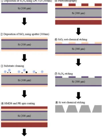
The microhole structures were manufactured on Si(100) wafers (thickness, 300 µm). Both sides of the substrate were polished, because the solution can easily permeate into a rough surface. Fig. 1 outlines the steps of wet-chemical etching. Three layers were deposited on the Si(100) before pattern formation. The first, a 200 nm thick silicon nitride layer, was obtained by low-pressure chemical vapour deposition (LPCVD, step 1). A 300 nm thick silicon dioxide layer was then RF sputtered (step 2). In order to etch the Si substrate, a pattern mask layer must be formed. Generally, if a commonly used SiO2 layer is selected, it reacts with KOH solu- tion which is etchant of the Si substrate. Therefore, we chose Si3N4as the middle layer because it does not react with KOH solution and also the etchant H3PO4of Si3N4
matters little to Si substrate. On the other hand, it is in use buffered oxide etchant to etch SiO2 and Si3N4 is not associated with buffered oxide etchant. Thus these are considered to be the most proper layers. The sub- strate was cleaned using acetone and methanol (step 3) before the third layer of hexamethyldisilazane (HMDS) and photoresist was added by spin coating for 40 s at 3500 rpm for the front side and 1500 rpm for the back (step 4). The pattern was then obtained by exposure and development (step 5). The SiO2 and Si3N4 layers were selectively etched by buffered oxide etchant (6:1) at room temperature and H3PO4(80%) at 160 – 170◦C in turn (steps 6 and 7). In the final stage (step 8), micro- holes formed in the Si(100) by wet etching with KOH (20%) at 70, 80, or 90◦C. The shapes and depths of the resulting microhole structures were investigated by field emission scanning electron microscopy (FE-SEM), and the etching mechanism was analysed via atomic struc- ture observations.
III. RESULTS AND DISCUSSION
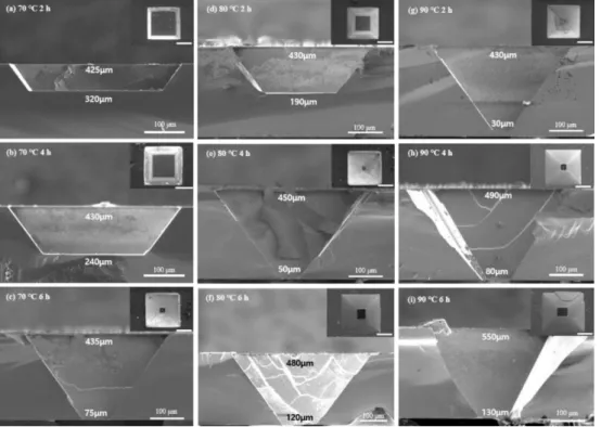
Fig. 2 shows cross-sectional FE-SEM images of the Si(100) after wet etching at different temperatures for
Fig. 1. (Color online) Outline of Si(100) wet-chemical etching.
various durations. Samples in the top (a, d, g), mid- dle (b, e, h), and bottom (c, f, i) rows in the figure were etched by KOH (20%) for 2, 4, and 6 h, respectively. The left (a–c), middle (d–f), and right (g–i) columns show samples etched at 70, 80, and 90 ◦C, respectively. All samples had surfaces indented at the same angle of 54.7◦, but etching reached different depths. The width of the pattern before etching was 400 µm in each case. The pat- tern size and substrate thickness determined the size of each hole. Etching accelerated with increasing tempera- ture. Holes through the substrate emerged after 6 h at 70
◦C, after 4 h at 80◦C, and after 3 h at 90◦C (the latter is not shown in Fig. 2). Under these conditions, the etch- ing depth exceeded the substrate thickness of 300 µm.
Fig. 3(a)–(c) represents the samples in Fig. 2, depicting the progression of etching at different temperatures: the holes became deeper and generally wider with time. The side etching rates at 70, 80 and 90 ◦C were on average 3, 11 and 20.25 µm/h, respectively. It was almost un- changed at 70◦C, but showed a sharp increase over 80◦C.
Fig. 2. Cross sectional FE-SEM images of Si(100) etched for (a) 2, (b) 4, and (c) 6 h at 70 ◦C; (d) 2, (e) 4, and (f) 6 h at 80 ◦C; and (g) 2, (h) 4, and (i) 6 h at 90◦C. The inset image is the top view of each picture and scalebar is 200 µm.
Fig. 3. (Color online) Progression of Si(100) etching at (a) 70, (b) 80 and (c) 90◦C. (d) Dependence of etching depth (left axis) and hole width (right axis) on etching duration.
Temperature can thus be set to control the width of the holes. Fig. 3(d) shows the relation between the etching time and depth (left axis, full symbols) and width (right
axis, hollow symbols) of the resulting holes. The etching rates at 70, 80, and 90◦C were 41, 73, and 143 µm/h, respectively, showing a substantial increase with temper-
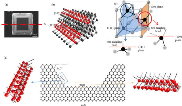
Fig. 4. (Color online) (a) FE-SEM images of Si(100) etched for 4 h at 70◦C. (b) Three-dimensional atomic schematic diagram of Si(100). (c) {100} and {111} plane lattices of a diamond structure. (d) Atomic diagram of the cross section of Si(100) and the lattice structures of the {100} and {111} planes.
ature. Atomic structure analysis helped to understand the etching process. Fig. 4(a) shows a top-view FE-SEM image of a Si(100) sample etched for 4 h at 70 ◦C, and Fig. 4(b) outlines the three-dimensional atomic structure of Si. Fig. 4(c) shows the diamond structure, which is adopted by Si crystals, and the shape of the lattice when it is cut along the {100} and 111 planes, which have two and one dangling bonds, respectively. Fig. 4(d) depicts the cross-sectional atomic structure of Si(100) when cut in the <011> direction. It clearly shows the hexago- nal pattern that appears spontaneously in the diamond structure. When the Si(100) is cut at 54.7◦, the {111}
plane emerges. Given that the {100} plane has two dan- gling bonds and the 111 plane has only one, the {111}
plane etches more slowly than the 100 plane owing to the larger activation energy needed to break the bonds behind the plane.
Si + 2OH− −→ Si(OH)2+2 + 4e− Si(OH)2+2 + 2OH−−→ Si(OH)4
Si(OH)4+ 4e−+ 4H2O−→ Si(OH)26−+ 2OH−+ 2H2
(1) Eq. (1) is the chemical reaction process of Si and KOH.
First, Si and OH−ions of KOH make Si(OH)2. This then
forms Si(OH)4, which reacts with H2O to give Si(OH)6
and H2. The Si is thus etched as Si(OH)6 dissolves in water [27].
IV. CONCLUSION
Microholes were formed in Si(100) wafers by wet- chemical etching with KOH (20%) solution at 70, 80 and 90◦C for different durations. This method does not re- quire expensive equipment or considerable time, and it can produce large numbers of microholes. Its sensitivity to time and temperature enables holes of specific depths and widths to be obtained in a relatively simple pro- cedure. The microhole structures fabricated using this process offer interesting functionalities and potential ap- plications as elements that form surface plasmons.
ACKNOWLEDGEMENTS
This research was supported by Basic Science Re- search Program through the National Research Founda- tion of Korea (NRF) funded by the Ministry of Education (No.2017R1A2B4009832).
REFERENCES
[1] B. Liedberg, C. Nylander and I. Lundstrom, Sens.
Actuators. 4, 299 (1983).
[2] A. J. Haes and R. P. Van Duyne, Anal. Bioanal.
Chem. 379, 920 (2004).
[3] M. A. Seo, J. H. Kang, H. S. Kim, J. H. Cho and J.
Choi et al., Sci. Rep. 5, 10280 (2015).
[4] Y. M. Bahk, B. J. Kang, Y. S. Kim, J. Y. Kim and W. T. Kim et al., Phys. Rev. Lett. 115, 125501 (2015).
[5] M. Najiminaini, F. Vasefi, B. Kaminska and J. J. L.
Carson, Appl. Phys. Lett. 100, 043105 (2012).
[6] C. Genet and T. W. Ebbesen, Nature Rev. 445, 39 (2007).
[7] A. Lesuffleur, H. Im, NC. Lindquist and SH. Oh, Appl. Phys. Lett. 90, 243110 (2007).
[8] J. Parsons, E. Hendry, C. P. Burrows, B. Auguie and J. R. Sambles et al., Phys. Rev. B. 79, 073412 (2009).
[9] T. Sannomiya, O. Scholder, K. Jefimovs, C. Hafner and A. B. Bahlin, Small 7, 1653 (2011).
[10] H. W. Huang, C. H. Lin, J. K. Huang, K. Y. Lee and C. F. Lin et al., Mater. Sci. Eng. B. 164, 76 (2009).
[11] W. Zhou, G. Min, Z. Song, J. Zhang and Y. Liu et al., Nanotechnology 21, 205304 (2010).
[12] S. Jeon, J. H. Jeong, Y. S. Song, W. L. Jeong and J. J. Kim et al., Nanoscale 6, 2642 (2014).
[13] Y. C. Kim and Y. R. Do, Opt. Express 13, 1598 (2005).
[14] J. H. Kim, J. K. Koh, B. G. Kim, J. H. Kim and E.
Y. Kim, Angew. Chem. 124, 6970 (2012).
[15] K. Q. Peng, X. Wang, L. Li, X. L. Wu and S. T.
Lee, J. Am. Chem. Soc. 132, 6872 (2010).
[16] S. E. Han and G. Chen, Nano Lett. 10, 1012 (2010).
[17] M. K. Kim, H. Sim, S. J. Yoon, S. H. Gong and C.
W. Ahn et al., Nano Lett. 15, 4102 (2015).
[18] F. Lacour, N. Courjal, M. P. Bernal, A. Sabac and C. Bainier et al., Opt. Mater. 27, 1421 (2005).
[19] J. Henzie, M. H. Lee and T. W. Odom, Nat. Nan- otechnol. 2, 549 (2007).
[20] M. H. Lee, M. D. Huntington, W. Zhou, J. C. Yang and T. W. Odom, Nano Lett. 11, 311 (2011).
[21] J. Chen, J. Shi, D. Decanini, E. Cambril and Y.
Chen et al., Microelectron. Eng. 86, 632 (2009).
[22] Z. Li, Y. Gu, L. Wang, H. Ge and W. Wu et al., Nano Lett. 9, 2306 (2009).
[23] K. Awazu, X. Wang, M. Fujimaki, T. Kuriyama and A. Sai et al., J. Vac. Sci. Technol. B 23, 934 (2005).
[24] H. I. Smith and M. L. Schattenburg, IBM J. Res Develop. 37, 319 (1993).
[25] Q. Guo, T. Tanaka, M. Nishio, H. Ogawa and X.
Mei et al., Jpn. J. Appl. Phys. 41, L118 (2002).
[26] S. Shingubara, O. Okino, Y. Murakami, H. Sakaue and T. Takahagi, J. Vac. Sci. Technol. B 19, 1901 (2001).
[27] H. Seidel, L. Csepregi, A. Heuberger and H. Baum- gartel, J. Electrochem. Soc. 137, 3612 (1990).