http://dx.doi.org/10.5369/JSST.2015.24.4.219 pISSN 1225-5475/eISSN 2093-7563
Transparent Conducting Multilayer Electrode (GTO/Ag/GTO) Prepared by Radio-Frequency Sputtering for Organic Photovoltaic’s Cells
Rina Pandey
1,3, Jung Hyuk Kim
1, Do Kyung Hwang
2,3, and Won Kook Choi
1,3+Abstract
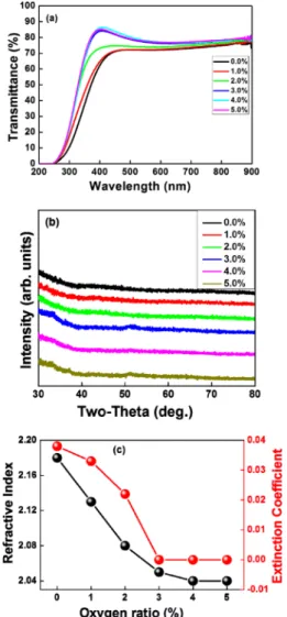
Indium free consisting of three alternating layers GTO/Ag/GTO has been fabricated by radio-frequency (RF) sputtering for the appli- cations as transparent conducting electrodes and the structural, electrical and optical properties of the gallium tin oxide (GTO) films were carefully studied. The gallium tin oxide thin films deposited at room temperature are found to have an amorphous structure. Hall Effect measurements show a strong influence on the conductivity type where it changed from n-type to p-type at 700
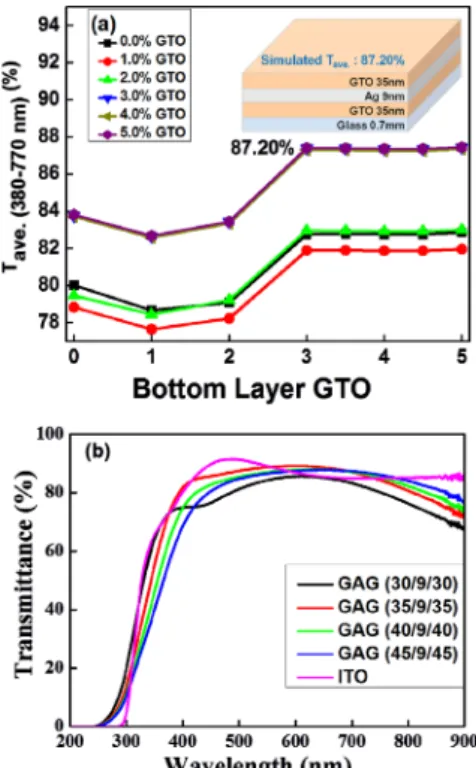
oC. GTO/Ag/GTO mul- tilayer structured electrode with a few nm of Ag layer embedded is fabricated and show the optical transmittance of 86.48% in the vis- ible range (λ = 380~770 nm) and quite low electrical resistivity of ~10
-5Ω cm. The resultant power conversion efficiency of 2.60%
of the multilayer based OPV (GAG) is lower than that of the reference commercial ITO. GTO/Ag/GTO multilayer is a promising trans- parent conducting electrode material due to its low resistivity, high transmittance, low temperature deposition and low cost components.
Keywords: Transparent conductive oxide, Gallium Tin Oxide (GTO), RF Sputtering, Structural and optical Properties, Bulk hetero-junction Organic Photovoltaic’s Cells (BHJ-OPVs), and power conversion efficiency
1. INTRODUCTION
Transparent conducting oxides (TCO) are the unique materials which possess low resistivity characteristics while maintaining high optical transparency. The inherent properties, transmittance and electrical conductivity of the TCOs are important factors which make them potential candidates for TCE applications such as plasma display panels, flat panel displays, touch panels, solar cells, organic light emitting diode, gas sensors and other optoelectronic devices [1]. The increased utilization of many transparent electrodes has accelerated the development of inexpensive TCO materials [2]. Indium tin oxide (ITO) is well known for TCO materials because of its excellent electrical and optical properties. However, due to the high cost and scarcity of
indium in TCO, there is urgent need of an alternative material with low cost and similar properties [3]. Zinc oxide film is cheaper than ITO but it shows the poor thermal stability. In contrast, Tin Oxide (SnO 2 ) film shows the best thermal and chemical stability which is inexpensive to manufacture and has good mechanical durability, but a high resistivity. SnO 2 is an n- type semiconductor with a wide band gap of approximately 3.7 eV [4-6]. Poor electrical conductivity can be improved by controlling stoichiometry or doping with impurities [7-12].
Researchers are dedicated to find new transparent conductive electrodes such as nanotubes, graphene, metal nanowires, dielectric-metal-dielectric (D/M/D) and related structures. D/M/D materials have been suggested as a candidate to overcome the limits of both the electrical and optical properties of single layer TCOs. It allows both the overall carrier concentration and the mobility to be increased, prevailing to some extent the limitation imposed by ionized impurity scattering in metal oxide single layers. In DMD structure, an insertion of metal layer as Ag [13], Ni [14], Cu [15] and Au [16] shows good conductivity.
Sandwiching a thin metal layer between two dielectric layers D/
M/D has been presented as an alternative approach to obtain the combined benefits of high transmission as well as the excellent conductivity of metals. Studies on a variety of multilayer electrodes [17-24] have been investigated for indium free transparent conducting oxides for organic photovoltaic’s cells.
Ellmer et al. recently published: either Ag nanostructures or D/M/
1
Materials and Life Science Division, Korea Institute of Science and Technology (KIST), Seongbuk Gu, Hwarangro 14 Gil 5, Seoul 136-791, Korea
2
Post Silicon Semiconductor Institute, Korea Institute of Science and Technology (KIST), Seongbuk Gu, Hwarangro 14 Gil 5, Seoul 136-791, Korea
3
Department of Nanomaterials Science and Engineering, Korea University of Science and Technology (KUST), Gajeongro 217, Yuseong-gu, Daejeon 305-350, Korea
+