2018년 1월
17ZB1200
전체부수
ETRI 주요 사업: 금속-절연체 전이 기술 개발
ETRI Principal Project: Project on Mechanism and application of
Metal-Insulator Transition
인 사 말 씀
ETRI 주요사업은 혁신형 국가 전략기술 개발을 위한 창의연구
수행을 통하여 세계 최고의 원천기술을 단계적으로 확보하고,
노벨상에 버금가는 연구결과 창출을 통한 World Top Class의
정부출연연구소의 위상 달성을 목표로 2016년부터 정부 출연금
사업으로 추진된 전략 사업입니다.
세부과제로 금속-절연체 전이(MIT) 현상규명 및 응용기술
개발을 수행하여 국제원천특허 획득 및 SCI 저널에 연구성과 게재
등의 결과를 가져왔으며, 각 분야 핵심원천기술 창출의 최종목표
달성에 다가가고 있습니다. 본과제가 목표대로 진행되기 위하여
연구가 심화됨에 따른 예산 및 제도적 지원체계를 갖출 수 있도록
더욱 노력할 것입니다.
향후 MIT 창의연구가 목표 이상의 성과를 거둬 물리학의 문제를
해결하여 국가의 위상을 세계 만방에 알리고 또한 미래 원천기술
확보를 통한 미래시장 선점 및 국가기술경쟁력 제고에 획기적으로
기여하고 ETRI 연구개발의 새로운 지평을 열기를 기대합니다.
2018년 1월
한국전자통신연구원 원장 이 상 훈
제 출 문
본 연구보고서는 주요사업인 " 금속-절연체 전이(Metal-Insulator
Transition:MIT) 기술 개발"의 결과로서, 본 과제에 참여한 아래의
연구팀이 작성한 것입니다.
2018년 1월
연구책임자 : 책임연구원 김현탁 (신소자연구그룹)
연구참여자 : 연 구 원 테티아나(신소자연구그룹)
연구참여자 : 연 구 원 조성우 (신소자연구그룹)
연구참여자 : 연 구 원 정순규 (신소자연구그룹)
연구참여자 : 연 구 원 최영규 (신소자연구그룹)
연구참여자 : 연 구 원 조진철* (신소자연구그룹)
연구참여자 : 연 구 원 손지민* (신소자연구그룹)
연구참여자 : 교 수 Dimitri N Basov**
(Columbia University: 국제공동연구)
연구참여자 : 연 구 원 Alex McLeod**
(Columbia University: 국제공동연구)
연구참여자 : 연 구 원 Aaron Sternbach**
(Columbia University: 국제공동연구)
* 연수생, 위촉연구원, 인턴 ** 공동연구기관요 약 문
Ⅰ. 제 목
ETRI
주요
사업,
금속-절연체
전이(Metal-Insulator
Transition:MIT) 현상규명 및 응용기술 개발
Ⅱ. 연구목적 및 중요성
본 연구의 목적은 물리학의 미해결 문제인 금속-전연체 전이
(MIT) 현상을 규명하여 인류발전에 기여한다. MIT 현상규명은 1930
년대에 금속의 자유전자들 사이에 강한 쿨롱 상호작용(Coulomb
interaction)이 존재하면 금속에서 부도체로 상전이 한다는 위그너
와 모트가 제안한 강상관 MIT 현상은 양자역학적으로 정밀하게 계산
이 되었지만 실험적으로 아직 증명되지 않은 물리문제이다. 그 후
MIT 근방에서 고온초전도, 절연파괴, 자이안트 마그넷티즘 등 새로
운 물리현상이 발견되었다. 또 공학적으로는 반도체 소자의 크기를
줄이면서 나타나는 단채널 효과 (Short channel effect)가 큰 문제로
대두되었다. 이 문제를 극복하기 위해 반도체 한계극복이라는 큰 이
슈가 등장하였고, 이 문제 해결의 대안으로 반도체보다 저항이 낮은
금속특성을 이용하는 절연체(부도체, Insulator)-금속(도체, Metal)
전이가 제안되었다. 본 연구는 학문적 중요성뿐만 아니라 기술적으
로도 새로운 패러다임을 바꾸는 반도체 한계를 극복하는 신기술을
창출하기 때문에 매우 중요하다.
Ⅲ. 연구내용 및 범위
금속-절연체 전이(Metal-Insulator Transition, MIT) 현상규명
및 MIT 나노기초 핵심응용 기술 개발을 통한 강상관 물질에서 MIT
현상을 연구하고, 핵심 응용소자로써 MIT 센서, 스위치 등을 연구한
다. 그리고 연구된 응용소자를 이용하여 관련 응용 기술 개발을 수
행한다. 또한 MIT 현상에 대한 국제공동연구를 수행함으로써 MIT 의
학문적 기초와 응용 기술을 더욱 깊이 있게 발전시키고자 한다.
Ⅳ. 연구결과
MIT 현상규명 연구: MIT 물질 VO2 에서 코히런트 포논의 온도의
존성을 조사하여 CDW 구조와 ZigZag 체인 구조를 갖는 M2 구조에서
구조 상전이를 겪지 않는 MIT 현상을 최초로 관측하였다.
ETRI-Columbia 국제공동연구로서 나노레벨에서 팸토초 기술로 MIT 현상을
측정할 때 발생하는 노이즈 문제를 해결하기 위하여
Transient-pseudo Heterodyne (Tr-pHD) 검출 방법을 개발하여 pHD 방법 보다
더 정밀한 이미지를 얻었다. 그리고 ETRI 가 개발한 Hole-driven MIT
이론을 물리문제 ‘감소하는 도핑에 따른 발산하는 유효질량’ 데이
터에 적용하여 발산하는 유효질량의 정체를 밝혀내므로서 30 년 미해
결 문제 ‘high-Tc Superconductivity’메카니즘을 밝혔다.
MIT 응용연구: Si 소자에서 제너의 턴넬 점프(양자 점프) 현상
을 제어하는 신개념을 발견하였다. MIT 물질의 VO2 에서 약간의 산소
를 더 넣었을 때 VO2.3 의 물질이 만들어 진다. 그런데 그 물질의 에
너지 밴드가 초록광에 중심 피크를 가지면서 노랑색 파랑색으로 에
너지 밴드 폭을 갖는다. 이것은 가시광을 측정할 수 있다는 힌트를
가지고 백색광 검출실험을 하여 조도센서를 만들 수 있었다. 기존의
Si 반도체 센서보다 저럼한 센서가 되어 상용화가 기대된다. 그리고
MIT-CTS (Critical Temperature Switch)를 이용하여 무선화재 감지기
를 개발한다. IOT (Internetof Things) 통신을 위해 무선 감지기와
감지기 사이를 통신하는 매시 넷트웍을 연구하였다. 그리고 MIT 기
술 사업화를 위하여 시장상황에 맞는 보다 저렴한 연기감지기를 개
발중이다.
Ⅴ. 기대성과 및 건의
금속-절연체 전이 현상규명 연구를 통하여 물리학의 미해결 문
제를 풀어서 인류의 발전에 한국인의 우수성을 국제적으로 알려 국
가위상을 향상시키는데 기여한다. MIT 응용기술로서 턴넬 점프 소자,
조도센서, CTS-이용 무선화재감지기 및 매시 넷트웍, 고성능 연기감
지기를 개발 상용화 하여 그 분야에서 기술적 발전뿐만 아니라 수출
을 하여 국부창출에 기여하도록 한다.
ABSTRACT
Ⅰ. TITLE
ETRI Principal Project: Project on Mechanism and application
of Metal-Insulator Transition
Ⅱ. THE OBJECTIVES
Metal-insulator transition (MIT) is a topic for research
interest in the field of condensed matter physics. Experimental
and theoretical studies to reveal the mechanism of MIT have been
on-going issue for half a century and are necessaries to be
clarified. Moreover, future devices using electrical jump are
required due to small size of devices and low power. This project
study new concept devices of using jump amd makes their
applications.
Ⅲ. THE CONTENTS AND SCOPE OF THE STUDY
As for researches of the MIT mechanism, the MIT is studied
by observing the MIT and the structural phase-transition
phenomena through measuring coherent phonons using Femtosecond
technique in a strongly correlated VO
2which has two insulating
substructures of the CDW (Charge Density Wave) and zigzag chain.
Moreover, in the MIT measurement system of nanolevel and
femtosecond measuring speed, a research reducing of a lot of
noise is performed through ETRI-Columbia collaboration. A
diverging effective mass in a superconducting material related
to the mechanism of high-T
csuperconductivity is explained using
the hole-driven MIT theory ETRI developed.
different from the MIT jump is observed and its application is
considered. A research on a visible sensor using VO
2.3is explained.
A wireless fire alarm detector using the MIT CTS device is
developed and a mesh network is also researched to connect the
wireless detectors. Furthermore, for transfer of the MIT
technologies, a high performance smoke detector, using the
visible detector and fitting the market situation, is developed.
Ⅳ. RESULTS
For the MIT-mechanism researches, we measured a difference
between the CDW and the zigzag chain insulating substructures in
M2 of VO
2for the temperature dependence of coherent phonons. The
phonos of the chain structure disappeared prior to the those of
the CDW, which indicates the first observation of the Mott
transition. As for the noise problem in nearfield image, a
detection method of a transient pseudoheterodyne rather than the
heterodyne method made a detail nearfield image. A physics problem,
the identity of the diverging effective mass was clarified by
fitting of the hole-driven MIT heory. This resolved the mechanism
of high-T
csuperconductivity, which is known as a problem for 30
years.
For the MIT application researches,a new current jump was
observed, which differs from the MIT jump. It was interpreted
that it is the Zener’s tunnel jump appearing through the pn
junction and is controlled by a managing terminal. We say that
this is a quantum-jump transistor. The VO
2.3samples measured the
visible light. It is used as a visible dection sensor cheaper
than a silicon visible sensor. The wireless fire detector possible
mesh network is developed using the MIT CTS sensor. Additionally,
a smoke detector using the visible sensor we developed is studied
for commerization.
Ⅴ. EXPECTED RESULT & PROPOSITION
Researches on the MIT mechanism can contribute to development
of studies in this MIT field and advertising of the
Korean’superiority. The MIT technologies can be applied to
development of sensor or switch systems and contribute to thei ㄴ r
commercialization.
CONTENTS
CHAPTER 1 ETRI PRINCIPAL PROJECT, PROJECT ON MECHANISMAND
APPLICATION OF METAL-INSULATOR TRANSITION ···· 24
SECTION 1 Research Outline ... 24
SECTION 2 Research Objectives ... 24
SECTION 3 Research Systems ... 25
SECTION 4 Report Contents ... 25
CHAPTER 2 METAL-INSULATOR TANSITION MECHANISM ··· 26
제 1 절 Mott transition in chain structure of strained VO2
films revealed by coherent phonons ... 26
제 2 절 Artifact free time resolved near-field spectroscopy of
VO
2... 41
제 3 절 Analyzing diverging effective mass in YBa
2Cu
3O
6+xfor
high-Tc mechanism and pairing symmetry ... 47
제 3 장 APPLICATION OF METAL-INSULATOR TRANSITION ··· 64
제 1 절 Research of zener-tunneling-switch ... 64
제 2 절 Illuminance sensor and application using VO
2.3... 66
제 4 절 Smoke Alarm using a VO
2.3sensor ... 94
제 4 장 RESEARCH RESULT ··· 96
1. Top 100 Research Award 2017 ··· 96
2. Publication ··· 96
3. Patents ··· 97
4. Presentation ··· 98
5. Technical Memo ··· 98
제 5 장 CONCLUSIONS AND SUGESTIONS ··· 101
제 1 절 Conclusions ... 101
목 차
제 1 장 ETRI 주요 사업, 금속-절연체 전이(METAL-INSULATOR
TRANSITION:MIT) 현상규명 및 응용기술 개발 과제 ·· 24
제 1 절 사업 개요 ... 24
제 2 절 사업 목표 및 내용 ... 24
제 3 절 사업 수행 체계 ... 25
제 4 절 보고서 체계 ... 25
제 2 장 2017 년 금속-절연체 전이 현상규명 및 관련 연구 ··· 26
제 1 절 Mott transition in chain structure of strained VO2
films revealed by coherent phonons ... 26
제 2 절 Artifact free time resolved near-field spectroscopy of
VO
2... 41
제 3 절 Analyzing diverging effective mass in YBa
2Cu
3O
6+xfor
high-Tc mechanism and pairing symmetry ... 47
제 3 장 금속-절연체 전이 응용기술 ··· 64
제 1 절 제너 터넬 점프 스위칭 기술 연구 ... 64
제 2 절 바나듐 산화물(VO
2.3)을 이용한 조도센서의 제작과 특성 측
정 ... 66
제 3 절 CTS 를 이용하연 무선 화재 감지기 제작 ... 80
제 4 절 바나듐 산화물(VO
2.3)을 이용한 연기감지기 ... 94
제 4 장 연구성과 ··· 96
1. 2017 년 국가연구개발 우수성과 ··· 96 2. 논문 ··· 96 3. 특허 ··· 97 4. 학회발표 ··· 98 5. TM 문서 ··· 98 6. 국제홍보 ··· 100제 5 장 결론 및 건의사항··· 101
제 1 절 결론 ... 101
1. 금속-절연체 전이 현상규명 성과 ··· 101 2. 금속-절연체 전이 응용 기술 개발 성과 ··· 103제 2 절 건의사항 ... 104
표목차
표 2-1. 각 측정방법에 따른 전류값 변화 ... 79 표 3-1.기존 화재감지기와 CTS 를 이용한 무선화재감지기의 소비전류 비교 ... 89
그림목차
그림 1-1. 사업 수행 체계 ··· 25 그림 2-1. (A) TEMPERATURE DEPENDENCE OF RESISTANCE OF THE STRAINED 120
NM THICK VO2 FILM ON AN ALN/SI SUBSTRATE. AN INSULATOR-TO-METAL
TRANSITION TEMPERATURE (TIMT) IS APPROXIMATELY 350 K, WHICH IS 10 K
HIGHER THAN TIMT OF THE BULK SAMPLE. (B) NORMALIZED PROBE
REFLECTIVITY (R/R0) AT PUMP POWERS OF 0.9 MW (2.1 MJ/CM2) AND 1.8 MW
(4.2 MJ/CM2) MEASURED AT DIFFERENT TEMPERATURES OF VO
2/ALN/SI. (C)
HRTEM IMAGE OF THE VO2/ALN CROSS-SECTION WITH TWO FFT PATTERNS
FROM THE DIFFERENT VO2 STRUCTURES M1 AND M2 (WHITE DASHED
SQUARES) OBSERVED AT ROOM TEMPERATURE. (D, E) MAGNIFIED WHITE-DASHED AREA OF M1 AND M2 TAKEN FROM (C) AND MODELED STRUCTURES ALONG [010]M1 GROWTH DIRECTION AND [100]M1 ZONE AXIS FOR M1-VO2
AND [001]M2 GROWTH DIRECTION AND [110]M2 ZONE AXIS FOR M2-VO2. (F)
TOP VIEW OF THE IN-PLANE ALIGNMENT OF THE M1 (SKY-BLUE-COLORED
AM1 AND CM1 AXES), M2 (GREEN-COLORED AM2 AND BM2 AXES) AND R
(RED-COLORED BR AND CR AXES) PHASES OF VO2 WITH RESPECT TO ALN
(DARK-BLUE-COLORED TETRAHEDRAL UNIT CELLS WITH AALN AND BALN LATTICE
CONSTANT AND DALN – SHORT DIAGONAL OF TWO ALN UNIT CELLS USED
FOR CALCULATIONS IN (H). DASHED AREAS MARK THE UNDERLYING ALN SURFACE COVERED BY VO2 IN DIFFERENT PHASES (M1, M2 AND R), USED FOR
THE FILM-SUBSTRATE IN-PLANE AREA MISMATCH CALCULATIONS (G, H). ··· 31 그림 2-2. (A) TEMPERATURE DEPENDENCE OF TRANSIENT REFLECTIVITY WITH THE
EXTRACTED COMPONENT OF COHERENT PHONONS (INSET) FOR THE VO2/ALN/SI SAMPLE. (B) TEMPERATURE-FREQUENCY MAP OF THE FIVE
RED-DOTTED CURVE FROM 그림 2-1B, SIMULTANEOUSLY REVEALING THE STRUCTURAL AND ELECTRONIC STATES OF VO2 ON ALN/SI. (C-E)
REPRESENTATIVE FFT SPECTRA OBTAINED AT DIFFERENT TEMPERATURES. INSET OF 그림 2-2C SHOWS AN EXAMPLE OF THE LORENZIAN FUNCTION FITTING OF THE FFT SPECTRUM TAKEN AT 303 K. INSET OF 그림 2-2D
SHOWS THE BAND DIAGRAMS FOR THE SEMICONDUCTING (OR INSULATING) VO2 WITH THE CDWM2 AND ICM2 SUBSTRUCTURES (BEFORE IMT) AND FOR
THE SEMICONDUCTING (OR INSULATING) CDWMMP AND METALLIC MCMMP SUBSTRUCTURES (AFTER IMT). ··· 34 그림 2-3. WAVELET TRANSFORM CHRONOGRAM OF COHERENT PHONONS IN
THE VO2 FILM AT DIFFERENT TEMPERATURES. BLACK DASHED LINES SHOW
PHOTOINDUCED SOFTENING OF THE HIGHER FREQUENCY PHONONS, WHILE WHITE ARROWS MARK THEIR TEMPERATURE-INDUCED DAMPING. ··· 36 그림 2-4. ARRANGEMENT OF V-ATOMS IN DIFFERENT VO2 CRYSTALLINE
STRUCTURES. (A) THE MONOCLINIC INSULATING M1 WITH COMMENSURATE CHARGE-DENSITY-WAVE (CDWM1) SUBSTRUCTURES OF METAL ATOMS
DIMERIZED ALONG THE AM1 AXIS. M1 IS COMPOSED OF IDENTICAL DIMER
CHAINS OF TILTED V-ATOMS WITH A BOND LENGTH OF 2.628 Å AND AN INTERDIMER SPACING OF 3.172 Å. (B) THE MONOCLINIC INSULATING M2 WITH TWO TYPES OF ATOMIC SUBSTRUCTURES: THE COMMENSURATE CDWM2
WITH PERIODICALLY PAIRED ATOMS AND THE INSULATOR CHAIN ICM2 WITH
EQUALLY SPACED UNPAIRED V-ATOMS. (C) A MONOCLINIC METALLIC PHASE (MMP), WHICH IS STRUCTURALLY IDENTICAL TO M2 BUT WITH A METALLIC CHAIN MCMMP. (D) THE RUTILE METALLIC STRUCTURE WITH IDENTICAL RMET
SUBSTRUCTURES OF EQUALLY SPACED V-ATOMS. ONGOING CONFRONTATION OR “CROSSED SWORDS” BETWEEN MOTT (ELECTRON-CORRELATION (E-E)
-DRIVEN-IMT IN THE SAME STRUCTURE: M2↔MMP) AND PEIERLS
(STRUCTURALLY (E-PH)-DRIVEN-IMT IN DIFFERENT STRUCTURES: M1↔R) NATURES OF THE TRANSITION IN VO2. THE MOTT IMT (IC → MC) TAKES
PLACE BETWEEN (B) AND (C). THE SPT OCCURS BETWEEN (C) AND (D) DUE TO MELTING OF THE CDWMMP STRUCTURE. ··· 38
그림 2-5. 왼쪽그림은 AFM 으로 측정된 이미지이고, 가운데는 일반 PHD 방법으로 측정된 것이며, 오른쪽은 본 개발의 TRANSIENT-PHD 검출방법으로 측정된 것 임. 오른쪽 이미지가 가운데 이미지보다 정밀함을 알 수 있음. ··· 41 그림 2-6. INFRARED TIME-RESOLVED NANO-IMAGING EXPERIMENT AND RESULTS.
A) DIAGRAM SHOWING THE EXPERIMENTAL APPARATUS. THE ULTRAFAST PROBE BEAM (PURPLE) IS FOCUSED ONTO THE APEX OF AN AFM PROBE AT A PRECISE TIME DELAY FOLLOWING A PERTURBATION CAUSED WITH A SECOND ULTRAFAST PUMP BEAM (RED). STATIC INFRARED IMAGE, WHICH WAS
COLLECTED WITH THE TR-PHD METHOD USING THE 5TH HARMONIC OF THE TIP-TAPPING FREQUENCY WITH A PULSED LASER SOURCE. THIS IMAGE WAS OBTAINED ON A REPRESENTATIVE 10X10 ΜM2 REGION. THIS IMAGE REVEALS
METALLIC REGIONS (GOLD) DUE TO THE COMPRESSIVE STRAIN OF THE SUBSTRATE AS WELL AS INSULATING REGIONS (BLUE), WHERE THE FILM IS STRAIN RELIEVED. B) TR-SHD RESULTS OBTAINED ON THE VO2/TIO2 [001]
SAMPLE IN A 5X5 ΜM2 REGION AT THE PUMP PROBE TIME DELAY T
PS = 300
PS. C) TR-PHD RESULTS OBTAINED ON THE VO2/TIO2 [001] SAMPLE IN A 5X5
ΜM2 REGION AT THE SAME TIME DELAY AS IN PANEL (B). ··· 45
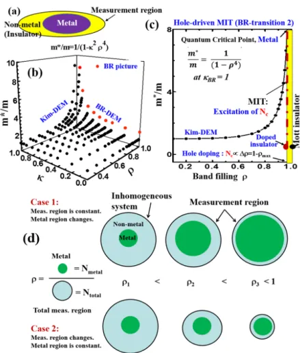
그림 2-7. THE EXTENDED BR PICTURE. (A) THE CONCEPT DRAWING OF AN
INHOMOGENEOUS TWO PHASE MODEL. IN THE MEASUREMENT REGION, THE VIOLET REGION IS METAL, AND THE YELLOW REGION IS NON-METAL OR INSULATOR. (B) EQ. (1) SHOWS TWO DIVERGENCES OF THE BR
DIVERGING-EFFECTIVE MASS (BR-DEM, RED-BULLETS) AT ρ=1 AND THE KIM-DEM AT
κBR=1. (C) THE DRAWING OF EQ.(1) AT κBR=1 SHOWS THE HOLE-DRIVEN MIT (BR-TRANSITION 2). THE YELLOW PORTION REPRESENTS THE
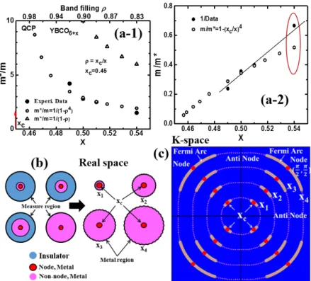
SEMICONDUCTOR REGIME AND ∆ρ AT RED DOT CORRESPONDS TO HOLE DOPING AND THE IMPURITY DOPED INSULATOR. THE METAL-INSULATOR TRANSITION (MIT) IS SHOWN AT RED DOT LINE BETWEEN THE DOPED INSULATOR AND METAL SPECIFYING EXCITATION. NC ≡ NC∝ ∆ρ WHICH IS THE DOPING CONCENTRATION FOR THE MIT. THE QUANTUM CRITICAL POINT IS GIVEN AT THE TRANSITION POINT. (D) TWO KINDS OF PERCOLATIONS ARE DESCRIBED. ρ IN TWO CASES IS THE SAME. ··· 52 그림 2-8. THE FITTING OF THE DIVERGING EFFECTIVE MASS (DEM). (A-1) THE
DEM DATA (BLACK DOT) EXTRACTED FROM QUANTUM OSCILLATION DATA IN 그림 2-9C BY SEBASTIAN, ET AL., [19] ARE CLOSELY FITTED BY EQ. (1) WHEN
κBR=1. UPPER X AXIS IS EXPRESSED AS A FUNCTION OF BAND FILLING ρ. QCP MEANS THE QUANTUM CRITICAL POINT. (A-2) THE INVERSE EFFECTIVE MASSES, M/M*, OF FIG. (A-1) ARE SHOWN. AT X=0.54 FAR FROM THE TRANSITION POINT, THE FITTING OF EQ. (1) WAS SLIGHTLY DEVIATED FROM THE EXPERIMENTAL DATA SHOWING THE LINEAR BEHAVIOR; THE DATA MAY HVE A LARGE EXPERIMENTAL ERROR. (B) A SCHEMATIC PERCOLATION DIAGRAM SHOWING AN INCREASE OF METAL REGION (PINK) WITH X (LEFT FIGURE CORRESPONDING TO CASE 1 IN 그림 2-7D). BASED ON ρI=XC/XI, AS X (PINK) INCREASES, SUCH AS X1≈0.49 < X2≈0.50 < X3≈0.51 < X4≈0.54 [19],
ρ=(RED/PINK) DECREASES (RIGHT FIGURE CORRESPONDING TO CASE 2 IN 그 림 2-7D); ρ1>ρ2>ρ3>ρ4 WITH RESPECT TO X1<X2<X3<X4 IS A PERCOLATION. THE EXTENT OF THE METAL REGION (RED DOT) AT THE NODE IS CONSTANT BECAUSE THE NUMERATOR OF ρ IS XC. (C) A SCHEMATIC FIGURE OF THE
FERMI POINT AND SURFACE IN K-SPACE BASED ON AN ANALYSIS OF 그림 2-8A AND B. BECAUSE THE EXTENT OF THE METAL REGION (PINK REGION) INCREASES AS X INCREASES (그림 2-8B), IN K-SPACE, THE FERMI SURFACE GROWS FROM THE FERMI POINT AT THE NODE (RED DOT) TO THE FERMI ARC (PINK ARC) AT THE ANTI-NODE. HOWEVER, THE MAGNITUDE OF THE FERMI POINT AT THE NODE (RED DOT) IS CONSTANT IRRESPECTIVE OF INCREASING OF X. THERE IS NO FERMI ENERGY (OR DOT OR SURFACE) AT THE ANTI-NODE (0, π). ··· 55 그림 2-9. D-WAVE MIT. (A) THE PSEUDOGAP AT THE ANTI-NODE. ARPES SPECTRA
MEASURED AT 10 K FOR HOLE-DOPED NON-SUPERCONDUCTING SINGLE CRYSTALS (Y=6.35, 6.45, 6.60) OF YBCOY. PSEUDOGAPS OF APPROXIMATELY -0.2 EV ARE CLEARLY SHOWN AT THE X AND Y ANTINODES (INVERSE BOLD TRIANGLES ▼, ▼, ▼). THE VALUE IS INDEPENDENT OF HOLE DOPING. THIS WAS CITED FROM FIGURE 4.3 IN YAGI’S PHD PAPER [30]. (B) THE D-WAVE MIT FROM THE PSEUDOGAP TO THE METAL AT THE NODE. ARPES SPECTRA MEASURED AT 10 K AT THE NODE FOR LIGHTLY DOPED SINGLE CRYSTALS OF YBCOY WITH Y=6.25 (PSEUDOGAP OF -0.1 EV), 6.30, 6.35, AND 6.40, WITHOUT
TC. THIS DATA WAS CITED FROM FIGURE 5.1 IN YAGI’S PHD PAPER [30]. (C) THE DOPING DEPENDENCE OF PSEUDOGAPS IN 그림 2-9(A) AND (B). AS Y INCREASES, THE PSEUDOGAP AT THE ANTI-NODE REMAINS UNCHANGED (FIG. A), WHILE THE EDGE OF THE PSEUDOGAP (WHITE ARROWS, BOTTOM FIGURES IN FIG. B) DECREASES AT THE NODE. THE MIT OCCURS AT THE NODE (D-WAVE MIT). THIS SHOWS THAT THE PSEUDOGAP HAS THE D-WAVE
SYMMETRY. ··· 56 그림 2-10. A MECHANISM FOR THE FORMATION OF THE SUPERCONDUCTING NODE GAP. THE DX2-Y2ELECTRONIC STRUCTURE CAN BE FORMED WHEN THE
METAL-INSULATOR TRANSITION (MIT) OCCURS AT THE NODE IN AN
ISOTROPIC PSEUDOGAP STRUCTURE (BLUE DASHED RING). THE SMALL PINK CIRCLES IN THE LARGE PINK CIRCLE ARE REGARDED AS THE NODAL FERMI POINTS MADE BY THE D-WAVE MIT NEAR DOPING XC. THE PINK CIRCLE IS THE FERMI SURFACE FORMED BY INCREASED DOPING. THE RED-DASHED ARROW INDICATES THAT BOUND CHARGES IN THE PSEUDOGAP POTENTIAL AT THE NODE ARE EXCITED TO THE FERMI ENERGY, DUE TO THE D-WAVE MIT (CONCEPTUAL INDICATION). THE SMALL GREEN CIRCLES IN THE LARGE GREEN CIRCLE ARE SUPERCONDUCTING INTRINSIC GAPS AT THE NODE WHEN THE NODAL FERMI POINTS BECOME A SUPERCONDUCTOR (PINK CIRCLE -> GREEN CIRCLE) [13,15]. THE GREEN RING IS THE ISOTROPIC SUPERCONDUCTING S-WAVE-LIKE GAP RESULTING FROM THE FERMI ARC AT OPTIMAL DOPING. IF THE SUPERCONDUCTING ENERGY GAP HAS D X2-Y2-WAVE-PAIRING SYMMETRY, THE D-WAVE-MIT SHOULD OCCUR AT THE ANTI-NODE. HOWEVER, THIS RESEARCH DOES NOT SUPPORT THE D-WAVE PAIRING SYMMETRY. THE CONSTANT MAXIMUM CARRIER DENSITY AT THE NODAL FERMI POINT (OR VELOCITY) WAS FIRST DISCLOSED [13]. ··· 57 그림 2-11. IMAGES OF TRAPPED MAGNETIC FLUX. (A) AND (B) THE HALF
MAGNETIC FLUX IMAGED BY A SQUID MICROSCOPE AT AN UNDERDOPED YBCO SUPERCONDUCTING RING ON THE TRICRYSTAL SUBSTRATE.
ANISOTROPY IS SHOWN, WHICH IS DENYING OF D-WAVE SYMMETRY. THESE WERE CITED IN THE TSUEI AND KIRTLEY’ S PAPER [36]. (E) FLUX IMAGE OF RING TYPE MEASURED IN AN OPTIMAL-DOPED SINGLE-LAYER TETRAGONAL TL2BA2CUO6+δ SUPERCONDUCTING RING WITHOUT A JUNCTION [37]. THIS
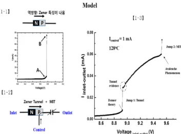
WAS CITED IN THE TSUEI’S PAPER [37]. ··· 59 그림 3-1. 그림 (1-1)은 제너의 브렉다운 현상임. 그림 (1-2)는 그림(1-3)의 데이터
를 설명할 수 있는 양자트랜지스터 모델이고, 그림 (1-3)은 양자 트랜지스터의 특성 데이터임. (1-3)에서 점선원은 NDR (NEGATIVE DIFFERENTIAL RESISTANCE)현상으로 턴넬 현상이 나올 때 나타나는 특성임. 이 NDR 은 에자 키 레오나가 노벨물리학상을 받았음. ··· 65 그림 3-2. 양자 트랜지스터의 특성 데이터. 양자 트랜지스터는 인렛, 아울렛, 콘트 롤 단자로서 콘트롤 단자로 흐르는 전류가 증가할수록 전류 점프의 크기와 점 프 전압이 감소함. 붉은색 원은 점프가 턴넬한 증거로서 NDR(NEGATIVE DIFFERENTIAL RESISTANCE) 현상을 보여줌. ··· 65
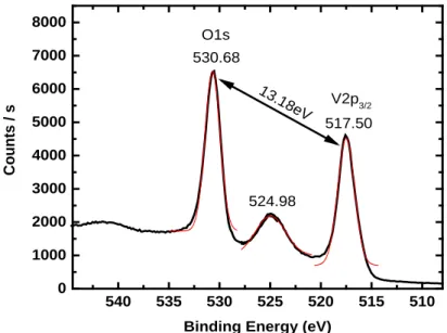
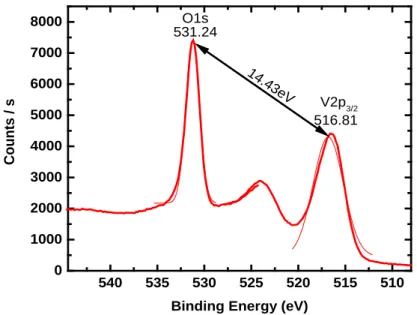
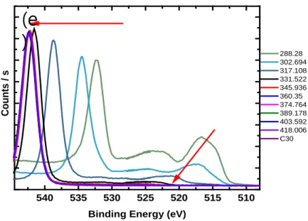
그림 3-3. VO2.3/AL2O3의 XPS DEPTH PROFILING 측정 그래프 ··· 68
그림 3-4. VO2.3/AL2O3의 XPS DEPTH PROFILING 표면 측정 ··· 68
그림 3-5. VO2.3/AL2O3의 XPS DEPTH PROFILING 표면으로부터 15 초간 에칭 데이 터 ··· 69
그림 3-6. VO2.3/AL2O3의 XPS DEPTH PROFILING 표면으로부터 30 초간 에칭 데이 터 ··· 69
그림 3-7. VO2.3/AL2O3의 XPS DEPTH PROFILING 표면 아래의 안정된 상 ··· 70
그림 3-8. VO2.3/AL2O3의 XPS DEPTH PROFILING AL2O3 기판과 박막의 계면 ··· 70
그림 3-9. . VO2.3/AL2O3의 원자농도 비율··· 71
그림 3-10. VO2.3/SI 의 XPS DEPTH PROFILING 측정 그래프 ··· 72
그림 3-11. VO2.3/SI 의 XPS DEPTH PROFILING 표면 측정 데이터 ··· 72
그림 3-12. VO2.3/SI 의 XPS DEPTH PROFILING 표면으로부터 15 초간 에칭 후 데이 터 ··· 73
그림 3-13. VO2.3/SI 의 XPS DEPTH PROFILING 표면 아래의 안정된 상··· 73
그림 3-14. VO2.3/SI 의 XPS DEPTH PROFILING SI 기판과 박막의 계면 ··· 74
그림 3-15. VO2.3/SI 의 원자농도 비율 ··· 74
그림 3-16. 완성된 VO2.3 소자의 개략도 ··· 75
그림 3-18. 완성된 샘플을 PCB 기판에 실버페이스트와 실버와이어를 이용하여 부 착한 모습··· 76 그림 3-19. 전극과 전극을 측정한 결과(그림 3-18 에서 수평형 2 단자구조) ··· 77 그림 3-20. 전극과 실리콘기판을 측정한 결과(그림 3-18 에서 수직형 구조) ··· 77 그림 3-21. 전극과 실리콘기판에 연결된 극성을 달리하여 측정한 결과(그림 3-18 에서 수직형 구조) ··· 78 그림 3-22. 전극과 전극에 연결된 극성을 달리하여 측정한 결과(그림 3-18 에서 수 평형 2 단자구조) ··· 78 그림 3-23. CTS 온도-저항 그래프 ··· 81 그림 3-24. 일반 화재감지기의 동작 순서도 ··· 82 그림 3-25. CTS 를 이용한 무선화재감지기 동작 순서도 ··· 83 그림 3-26. 무선 메쉬 네트워크··· 84 그림 3-27. CC2650 무선화재감지기 PCB ARTWORK ··· 86 그림 3-28.제작된 CTS 무선화재감지기 ··· 86 그림 3-29. NRF52832 를 이용한 무선화재감지기 PCB ARTWORK ··· 87 그림 3-30. NRF52832 로 제작된 무선화재감지기 ··· 88 그림 3-31.기존 무선화재감지기와 CTS 를 이용한 무선화재감지기의 소비전류 차이 측정 ··· 88 그림 3-32. API 서버 구성 ··· 90 그림 3-33. CTS 무선화재감지기 홈페이지 FRONT PAGE ··· 91 그림 3-34. CTS 무선화재감지기 웹페이지의 BUILDING LIST ··· 91 그림 3-35. CTS 무선화재감지기 웹페이지의 FLOOR PLANS ··· 92 그림 3-36. CTS 무선화재감지기 웹페이지의 EVENT LOG ··· 92 그림 3-37. 연기 감지기 다이어그램 ··· 94 그림 3-38.연기 감지기 내부 금형(암실) ··· 95 그림 3-39. 개발중인 연기 감지기 보드 ··· 95
그림 4-1. 2017 년 국개연구개발 우수성과··· 96 그림 5-1. TEMPERATURE-FREQUENCY MAP OF THE FIVE COHERENT PHONON
MODES (P1-P5, BLACK CIRCLES) WITH R/R0 RED-DOTTED CURVE ··· 101 그림 5-2. THE FITTING OF THE DIVERGING EFFECTIVE MASS (DEM). ··· 102 그림 5-3. 그림 (1-1)은 제너의 브렉다운 현상임. 그림 (1-2)는 그림(1-3)의 데이터 를 설명할 수 있는 양자트랜지스터 모델이고, 그림 (1-3)은 양자 트랜지스터의 특성 데이터임. (1-3)에서 점선원은 NDR (NEGATIVE DIFFERENTIAL RESISTANCE)현상으로 턴넬 현상이 나올 때 나타나는 특성임. 이 NDR 은 에자 키 레오나가 노벨물리학상을 받았음. 그림 1-3 에서 JUMP 1 이 양자 점프이고, 점프 2 는 MIT 점프이다. ··· 103
제 1 장 ETRI 주요 사업, 금속-절연체 전이(Metal-Insulator
Transition:MIT) 현상규명 및 응용기술 개발 과제
제1절 사업 개요
ETRI 창의연구실사업은 2012 년부터 2015 년까지 5 년간 수행되는 정부출연금 사업으로서, 2016 년부터 주요사업으로 변경되면서 그 사업속에서 “금속-절연체 전이 현상규명 및 응용기술 개발” 이라는 세부과제로 연구가 수행되었다제2절 사업 목표 및 내용
○ 최종연구목표 금속-전연체전이(MIT) 현상규명 및 MIT 신재료, 스위치 및 응용기술 개발 ○ 목표물리학의 문제 “금속-절연체 전이(Metal-Insulator Transition, MIT) 현상규 명”에 대해 국제공동연구를 포함해서 깊이 있는 연구를 수행하여 그 관련 물리 문제를 풀어서 일류의 발전에 기여한다. 또한 MIT 현상규명 기반 기초원천핵심 응용 기술을 개발하여 국가 산업발전에 이바지 하여 국부창출에 기여한다.
○ 연구내용
대표적인 모트 절연체 VO2에서 Mott MIT 에 관한 연구, 모트 MIT 규명을 위해
나노급 초고속 근접장 분광 기술 개발연구 (국제공동), 물리학의 30 년 문제인 고 온촌전도체 메커니즘 규명에 관한 연구, 양자점프 트랜지스터의 개념 연구, VO2.3
을 이용한 조도센서 연구, VO2 재료를 이용한 임계온도스위치를 이용한 무선화재
제3절 사업 수행 체계
그림 1-1. 사업 수행 체계제4절 보고서 체계
본 보고서는 제 1 장에서 주요 사업 개요, 목표, 추진체계를, 제 2 장에서는 금속-절연체 전이(Metal-Insulator Transition:MIT) 현상규명 및 관련연구 내용을, 3 장에서는 MIT 응용기술 개발에 관한 연구내용을, 4 장에서는 2017 년 수행한 연구 성과를 기술하며, 제 5 장에서는 결론 및 향후 발전을 위한 수행과정에서 나타난 문제점을 건의한다.제 2 장 2017년 금속-절연체 전이 현상규명 및 관련 연구
제1절 Mott transition in chain structure of strained VO2 films
revealed by coherent phonons
[한글요약][논문정보: nature 자매지, Scientific Report 7, 16038 (2017)] Mott 절연체에서 모트 금속-절연체 전이(MIT)는 고체 물리학의 오랜 물리문제 이다. 특히 구조상전이를 동반하지 않는 모트 MIT 는 구조 상전이를 동반하는 파이 얼스 MIT 와 함께 구분이 어려워서 혼돈을 거듭해왔다. 이 문제를 해결하기 위하여 대표적인 급격한 MIT 를 겪는 모트 절연체 VO2 에서 MIT 를 정밀하게 관측한다. VO2 는 2 개의 Substructures 로 구성되어 있다. 하나는 CDW 구조이고 다른 것은 ZigZag 의 equally Vanadium chain 구조이다. 체인 구조가 CDW 보다 먼저 MIT 가 일어나면 모트 MIT 라고 볼 수 있다. 이 현상을 초고속 측정 시스템을 이용하여 Coherent phonons 의 온도의존성을 측정한 결과 체인구조가 CDW 구조보다 먼저 MIT 가 일어 나는 것을 최초로 측정하였다 (그림 2-b). 이것은 모트 MIT 를 증명하는 중요한 실 험결과이다. 이 연구는 nature 자매지인 Scientic report 에 11 월에 게재되었다.
The characteristic of strongly correlated materials is the Mott transition between metal and insulator (MIT or IMT) in the same crystalline structure, indicating the presence of a gap formed by the Coulomb interaction between carriers. The physics of the transition needs to be revealed. Using VO2, as a
model material, we observe the emergence of a metallic chain in the intermediate insulating monoclinic structure (M2 phase) of epitaxial strained films, proving the Mott transition involving the breakdown of the critical Coulomb interaction. It is revealed by measuring the temperature dynamics of coherent optical phonons with separated vibrational modes originated from two substructures in M2: one is the charge-density-wave, formed by electron-phonon
(e-ph) interaction, and the other is the equally spaced insulator-chain with electron-electron (e-e) correlations.
Vanadium dioxide (VO2), a canonical transition metal oxide with strongly
correlated electrons, undergoes the insulator-to-metal transition (IMT) near TIMT = 340 K, accompanied by the structural phase transition (SPT) between the
monoclinic and rutile (R) phases. The IMT mechanism is still under debate, because the IMT occurs near the SPT and the complicated structure shields the driving mechanism of the phase transformation. It has been argued whether the IMT is the Mott transition driven by the breakdown of electron-electron (e-e) correlations, the Peierls transition induced by melting of the charge density wave (CDW) formed by electron-phonon (e-ph) interactions, or the Mott-Peierls transition occurring by means of both effects (e-e and e-ph). The microscopic understanding of the e-e and e-ph interactions, regarded as the IMT in doped semiconductors, Mott insulators, high temperature superconductors, layered transition metal dichalcogenides, is important for science and technology.
The VO2 below TIMT has the monoclinic structure (M1) and the second monoclinic
structure (M2) with two kinds of substructures of V-atoms, which are a CDW substructure with lattice distortion and an antiferromagnetic equally spaced insulator-chain (IC) one. The M2 phase, as an intermediate between M1 and R, was discovered in Cr-doped and strained VO2 samples. It enables the Mott IMT
scenario implying transformation from the IC to a metallic chain (MC), which occurs by excitation of charges in the indirect impurity band formed by such as oxygen vacancies leading to the chain collapse of the main band.
Numerous works have been published with both theoretical and experimental evidence for the metallization of the monoclinic phase and, thus, for the Mott transition. Among them, Tao, et al., monitored VO2 microbeams on heating using
techniques and showed that charge doping stabilizes a new monoclinic metal
phase prior to the SPT. Morrison, et al., used an ultrafast electron
diffraction technique with infrared transmissivity to separate the
optically-induced charge and lattice reorganizations in polycrystalline VO2 films.
Wegkamp, et al., performed femtosecond time-resolved photoelectron
spectroscopy of photoexcitated thin VO2 films and obtained an instantaneous
pure electronic transition excluding any structural bottleneck. J. Laverock, et al., observed a temperature-triggered Mott transition in VO2 with the help
of low-energy electron microscopy and photoemission spectroscopy. Li, et al., measured the monoclinic metallic phase under high pressure.
Despite intensive studies of the IMT, the two substructures in the monoclinic metallic phase (MMP), CDW and MC, have not been separately observed for the Mott transition. Moreover, the MC has never been experimentally proven. Thus, there has been no decisive argument for the Mott transition.
Here, we report a first observation of the metallic chain (MC) in the monoclinic structure of strained VO2 epifilms grown on an AlN/Si substrate,
providing strong evidence of the Mott transition. This is achieved by analyzing coherent phonons, measured below a photo-induced (thermal and non-thermal component) IMT threshold by ultrafast pump-probe spectroscopy. This is a unique tool capable of simultaneously sensing both structural reconstruction and electronic system transformation on a femtosecond timescale. Moreover, our results show that the dynamics of the phonons on heating reveal not only the structural reconstruction of VO2 during transitions of the M1 insulator → M2
insulator → Rutile metal, but also the intrastructural rearrangement of the V-chains in the M2 phase.
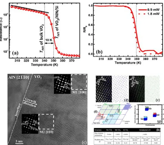
그림 2-1a shows the temperature dependence of electrical resistance for 120 nm thick VO2 film on AlN/Si with a critical transition temperature TIMT ≈
350 K higher than the typical value of bulk or bulk-like VO2 samples with TIMT
≈ 340 K. This is caused by the substrate-induced strain in the film, as
demonstrated by high resolution transmission electron microscopy (see 그림
2-1c-h), which stabilizes the insulating phase and, therefore, drives the
10 K-upshift of TIMT. As shown below, this peculiarity of the sample enables the extended existence of the monoclinic crystalline structure and its electronic insulator-to-metal switch at 350 K
그림 2-1b shows the temperature dependence of normalized probe reflectivity (R/R0) measured at two different pump powers, 0.9 and 1.8 mW, corresponding to the fluences of 2.1 and 4.2 mJ/cm2, respectively. Both R/R0 curves, in accordance with the resistance switching (그림 2-1a), exhibit the same drastic changes at about 350 K without any fluence dependence. Thus, the pump laser with a fluence up to 4.2 mJ/cm2 is low enough not to affect phase transition of the sample, in contrast to higher fluences. Further optical measurements, as presented in 그림 2-2, were performed at a pump fluence of 2 mJ/cm2.
그림 2-1c shows an HRTEM image with FFT patterns of the VO2/AlN
cross-section. The zone axis of the AlN substrate is defined as [21�1�0] (not shown). A prominent distinction in the V-atoms arrangement (see white dashed squares and adjacent FFT patterns) can be seen.
Careful analysis of the interplanar spacing and diffraction spot intensities reveals that these two areas represent two monoclinic phases of VO2: M1 and
M2. Magnified white dashed areas and modeled structures with growth directions of [010]M1 ([100]M1 zone axis) and [001]M2 ([110]M2 zone axis) are shown in
그림 2-1d and e.
그림 2-1f shows the schematic image based on the data extracted from the HRTEM image (그림 2-7c-e), depicting the in-plane alignment of VO2
M2 phases) and AlN (dark-blue-colored tetrahedral unit cells with aAlN lattice constant). Considering the lattice constants of AlN, M1-VO2, and M2-VO2, the
VO2 film is shown to be under in-plane tensile strains of approximately -7.2
and -13.2 % along aM1 and cM1, respectively, whereas it is stretched along aM2 by -2.5 % and compressed in the bM2 directions by +7.8 %. From the requirements of the minimal lattice constant mismatch at the film-substrate interface, the emergence of the M2 phase at room temperature is preferred. On the other hand, the formation energy of the M2 phase is slightly higher than that of M1, but the difference is blurred with increasing temperature.
Furthermore, the alignment of the monoclinic VO2, obtained from HRTEM (그림 2-1c), and the expected alignment (from crystallographic considerations) of the rutile (at high temperatures, after the structural phase transition) VO2
film on AlN substrate, result in the following film-substrate epitaxial relationship (그림 2-1f): (010)M1+(001)M2//(0001)AlN – at low temperatures, before SPT; (100)R//(0001)AlN – at high temperatures, after SPT. From this, the in-plane area of the VO2 unit cell for the M1, M2 and R phases, as well
as the respective area of the underlying AlN are calculated (see 그림 2-1h). The relative VO2/AlN in-plane area mismatch is shown in 그림 2-1g. The smallest
mismatch (-9.3 %, where “-” stands for stretched film by tensile strain from the substrate) is obtained for M2-VO2 on AlN, the intermediate (-16.0 %) – for R-VO2, and the largest (-20.1 %) – for M1-VO2. This explains the advantage
of the M2 phase, over M1, for the low-temperature VO2 film and the further
delay of the transition to the rutile phase, enabling the observation of the electronic transition into the monoclinic metal phase with two substructures.
그림 2-1. (a) Temperature dependence of resistance of the strained 120 nm thick VO2 film on an AlN/Si substrate. An insulator-to-metal transition temperature (TIMT) is approximately 350 K, which is 10 K higher than TIMT of the bulk sample. (b) Normalized probe reflectivity (R/R0) at pump powers of 0.9 mW (2.1 mJ/cm2) and 1.8 mW (4.2 mJ/cm2) measured at different temperatures of VO2/AlN/Si. (c) HRTEM image of the VO2/AlN cross-section with two FFT patterns from the different VO2 structures M1 and M2 (white dashed squares) observed at room temperature. (d, e) Magnified white-dashed area of M1 and M2 taken from (c) and modeled structures along [010]M1 growth direction and [100]M1 zone axis for M1-VO2 and [001]M2 growth direction and [110]M2 zone axis for M2-VO2. (f) Top view of the in-plane alignment of the M1 (sky-blue-colored aM1 and cM1 axes),
M2 (green-colored aM2 and bM2 axes) and R (red-colored bR and cR axes) phases of VO2 with respect to AlN (dark-blue-colored tetrahedral unit cells with aAlN and bAlN lattice constant and DAlN – short diagonal of two AlN unit cells used for calculations in (h). Dashed areas mark the underlying AlN surface covered by VO2 in different phases (M1, M2 and R), used for the film-substrate in-plane area mismatch calculations (g, h).
그림 2-2a shows the temperature dependence of transient reflectivity ΔR/R0 measured for VO2/AlN/Si. Here, at low temperatures of 303-323 K (blue and cyan
curves), the response of the sample to the pump stimulation is identical: near t = 0 (t is the time delay between the pump and the probe), ΔR/R0 undergoes a rapid negative offset due to electrons excitations by a pump energy of 1.6 eV (755 nm), which is higher than the energy gap of 0.6 eV. This rapid photoexcitation is followed by a few picoseconds of relaxation to a nonzero
thermalized state. Upon further heating (up to 347 K, 그림 2-2a), the
relaxation becomes increasingly suppressed, indicating the emergence of charge carriers that are supplied by metallic domains, which evolve with increasing
temperature. The latter is also demonstrated by 그림 2-1a, where at 340 K,
the resistance of VO2 drops faster than the exponential function, thus,
deviating from the Arrhenius law (marked by the black line) due to the coexistence of the insulating and metallic phases. Next, at 349 K, when the carrier concentration reached its critical value, a sign inversion of the initial ΔR/R0 offset occurs, indicating the overall electronic
insulator-to-metal transition (IMT) of VO2. Subsequent curves obtained at higher
Another important feature of the transient reflectivity signal (그림 2-2a) is oscillations with optical phonon frequencies, excited by femtosecond laser
pulses. The inset of 그림 2-2a shows the extracted coherent oscillations at
four different temperatures. Since the phonon modes are the signatures of the atom arrangement in the crystal lattice, their temperature dynamics trace the structural evolution of the sample. In order to reveal the crystallographic
transformations of the VO2 film in a frequency domain, the transient
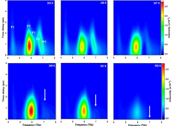
oscillations were processed by the fast Fourier transformation (FFT). The resulting temperature-dependent frequency map of the coherent phonons in VO2
is shown in 그림 2-2b and the representative FFT spectra are shown in 그림 2-2c-e.
그림 2-2b&c show five phonon modes at 4.38 THz (P1), 5.80 THz (P2), 6.07 THz (P3), 6.65 THz (P4) and 6.80 THz (P5) in the vicinity of room temperature (inset of 그림 2-2c exhibits the Lorentzian function fitting details). Among these, the P1, P2, and P4 phonons are consistent with those originated from the oscillations of V-atoms in the monoclinic M1 phase of VO2 having a 𝐶𝐶2ℎ5space
group, while P3 and P5 are from the monoclinic M2 phase with 𝐶𝐶2ℎ3 space group. Note that an observation of the P3 and P5 peaks from the M2 phase already
at 303 K is not typical for undoped VO2. This can be attributed to a
considerably strained state of the film, which is confirmed by high-resolution transmission electron microscopy (HRTEM) imaging of a VO2/AlN cross-section,
그림 2-2. (a) Temperature dependence of transient reflectivity with the extracted component of coherent phonons (inset) for the VO2/AlN/Si sample.
(b) Temperature-frequency map of the five coherent phonon modes (P1-P5, black circles) with R/R0 red-dotted curve from 그림 2-1b, simultaneously revealing the structural and electronic states of VO2 on AlN/Si. (c-e)
Representative FFT spectra obtained at different temperatures. Inset of 그림 2-2c shows an example of the Lorenzian function fitting of the FFT spectrum taken at 303 K. Inset of 그림 2-2d shows the band diagrams for the
semiconducting (or insulating) VO2 with the CDWM2 and ICM2 substructures
(before IMT) and for the semiconducting (or insulating) CDWMMP and metallic MCMMP substructures (after IMT).
Black circles in 그림 2-2b mark the precise values of the phonon frequencies, as determined by fitting of the FFT spectra (그림 2-2c-e). Tracing the temperature evolution of the phonon modes, the red shift of the P2-P5 phonons are observed in the vicinity of TIMT (in the range of 345-353 K) due to
heat-induced lattice expansion and phonon softening. Upon further heating (see 그림 2-2e), when more and more carriers are generated, the phonon vibrations become less pronounced and, above 359 K, they disappear due to the SPT to the rutile phase. The latter was also confirmed by in-situ temperature dependent X-ray diffraction measurements not shown here.
그림 2-2c-d show gradual reduction of the P2 and P4 peaks intensity on heating. The peaks are fully symmetrical Ag doublet phonons, associated with
stretching and tilting of dimerized V-V atoms in the M1 phase. This damping of the M1 peaks is accompanied by intensifying of the P3 peak from the M2 phase (그림 2-2d, curves at 347-349 K), suggesting the mutual transformation from M1 to M2 and, thus, dominance of the M2 phase at higher temperatures (at 347 K ≤ T < 359 K, 그림 2-2c-d). On the other hand, another M2 peak, P5, shows opposite to P3 tendency: its intensity continuously reduces on heating and finally, at 349 K (temperature corresponding to TIMT), when the P3 peak
reaches its maximum intensity, the P5 phonon totally vanishes.
To investigate the evolution of the electronic properties in time we have performed a wavelet analysis using VO2 oscillatory data measured at different
temperatures and using the Gaussian function 𝑓𝑓(𝑥𝑥) = 1
𝑤𝑤√2𝜋𝜋𝑒𝑒−(𝑥𝑥−𝑥𝑥𝑐𝑐)
2⁄(2𝑤𝑤2) with
𝑤𝑤 = 1𝑝𝑝𝑝𝑝.
그림 2-3. Wavelet transform chronogram of coherent phonons in the VO2 film
at different temperatures. Black dashed lines show photoinduced softening of the higher frequency phonons, while white arrows mark their temperature-induced damping.
그림 2-3 shows the representable frequency-time-intensity maps at different temperatures. It is seen that the phonon frequencies correspond to those obtained by FFT (그림 2-2b-e), but are some broader. Noticeable that, in the range of 303-349 K, the P5 peak from the insulating chain of M2 (ICM2) undergoes
a significant red shift from ~ 7.0 to ~ 6.7 THz with increasing time delay (shown by black dashed line). This behavior can be explained by a rapid pump-induced photoexcitation (please, see the ΔR/R0 offset at time delay ≤ 200
fs at 303-345 K in 그림 2-2a) of the d-electrons localized near V-ions composing the ICM2, thus, affecting their coherent vibrations.
However, in the FFT data (그림 2-2b-e) in the temperature range of 303-349 K, damping of the P5 peak by photoexcitations is not observed, because of insufficient time resolution. It became expressed only above 349 K (on the heat-induced insulator-to-metal transition): the P4 and P5 peaks intensities are strongly reduced due to scattering by charge carriers. On the other hand, at 347-349 K, the charge-density-wave P3 peak from M2 (CDWM2) becomes stronger
due to M1→M2 transition. Upon further heating, when more and more carriers are generated, the phonon vibrations become less pronounced and, above 359 K, they disappear (not shown) due to the SPT to the rutile phase. Thus, the results obtained by wavelet analysis are consistent with those, obtained by FFT (그림 2-2).
A striking discovery is strong damping of the higher frequency P5 phonons from M2 at TIMT ≈ 349 K and existence of the lower frequency P3 peak up to
357 K (그림 2-2, e). These can be explained by structural features of the M2 phase described below.
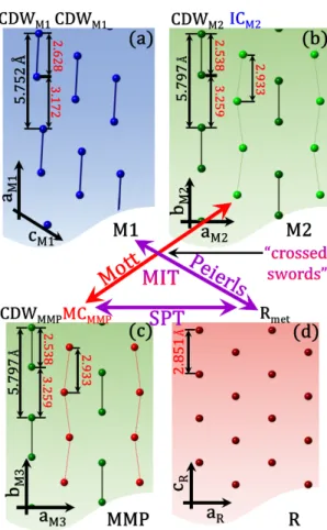
그림 2-4a shows the schematic of twisted V-V pairs in the M1 phase, which
can be considered as a superposition of two lattice distortions of M2. 그림
2-4b demonstrates the binary V-substructures in the M2 phase. One is the
commensurate CDWM2 (charge ordering in a distorted lattice) substructure with
straightened and alternately positioned metal atoms with spacings of both 2.538 Å between paired and 3.259 Å between unpaired V-V. The other is the
insulator-chain (ICM2) of a zigzag-like substructure with unpaired V-ions
positioned with an equal spacing of 2.933 Å, having strongly correlated localized electrons with the antiferromagnetic half spin.
그림 2-4. Arrangement of V-atoms in different VO2 crystalline structures. (a)
The monoclinic insulating M1 with commensurate charge-density-wave (CDWM1)
substructures of metal atoms dimerized along the aM1 axis. M1 is composed of
identical dimer chains of tilted V-atoms with a bond length of 2.628 Å and an interdimer spacing of 3.172 Å. (b) The monoclinic insulating M2 with two types of atomic substructures: the commensurate CDWM2 with periodically paired atoms
and the insulator chain ICM2 with equally spaced unpaired V-atoms. (c) A
monoclinic metallic phase (MMP), which is structurally identical to M2 but with a metallic chain MCMMP. (d) The rutile metallic structure with identical
“crossed swords” between Mott (electron-correlation (e-e)-driven-IMT in the same structure: M2↔MMP) and Peierls (structurally (e-ph)-driven-IMT in different structures: M1↔R) natures of the transition in VO2. The Mott IMT
(IC → MC) takes place between (b) and (c). The SPT occurs between (c) and (d) due to melting of the CDWMMP structure.
The Mott IMT was predicted to occur through the breakdown of the critical on-site e-e Coulomb repulsion in the IC and its transformation (그림 2-4c) from ICM2 to a metallic chain (MCMMP). Note that CDW substructure remains same
for M2 and MMP (CDWM2 ≡ CDWMMP). Inset of the 그림 2-2d shows the band diagram
before IMT for the semiconducting (or insulating) VO2 with the ICM2 and CDWM2
substructures and the band diagram after IMT for the metallic MCMMP and
semiconducting (or insulating) CDWMMP substructures
Based on the above considerations, the two types of observed phonons can be assigned to those coming from the M2 substructures as follows: the P5 phonon, disappearing at TIMT as a result of scattering by carriers generated at the
IMT, is regarded as that originating from the IC substructure (ICM2 in 그림
2-4b), while the P3 phonon, able to withstand the scattering effect up to
TSPT ≈ 359 K because fewer carriers are generated by the corresponding vibrating
V-atoms, is interpreted as that coming from the CDW substructure melting on the structural transition to the rutile phase (그림 2-4d). The long-living P3 phonon along with P1 and P2, all persisting up to 359 K, allow to prove that VO2 undergoes the Mott insulator-to-metal transition within the monoclinic
structure.
In conclusion, we have studied the temperature dependence of coherent phonons in strained VO2 films with monoclinic M2 phase stabilized in a wide temperature
explained by their scattering by charge carriers emerging when the zig-zag
insulating chain ICM2 substructure of M2, vibration of which creates
corresponding phonons, undergoes the Mott transition. While the lower-frequency phonons from the straight charge density wave CDWM2 substructure of
M2 persist up to TSPT (TSPT > TIMT). Thus, we were able the separate two kinds
of phonons from M2 and to obtain experimental evidence of the metallic chain (MC) in the monoclinic structure for the first time. This finding proves the Mott transition in VO2; it differs from suggestions that the VO2 insulator is
coupled to the charge order corresponding to the commensurate CDW state and that both e-e and e-ph interactions are crucial for the phase transition.
제2절 Artifact free time resolved near-field spectroscopy of VO
2[한글요약][논문정보: 13 Nov 2017 | OPTICS EXPRESS 25 (2017) 28589]
시험샘플에서 펨토초 나노급 근접장 측정을 할 때는 노이즈가 심해서 노이즈 를 줄이는 인공적 처리를 한다. 그런데 나노 분광기를 개발하는 과정에서 이것을 극복하는 기술을 개발하였다. 이것은 Transient pseudoheterodyne (Tr-pHD) 검출 방법이다. 이 방법을 사용하면 기존보다 훨씬 정밀한 측정이 가능하다. 이것은 나 노급 초고속 시스템을 개발할 때 필연적이다. 그래서 이번에 ETRI-콜롬비아와 공 동으로 개발하였다. 이 연구는 ETRI-Columbia 와 국제공동연구 계약을 맺고 수행한 연구 결과물이다. 그림 2-5. 왼쪽그림은 AFM 으로 측정된 이미지이고, 가운데는 일반 pHD 방법으로 측정된 것이며, 오른쪽은 본 개발의 Transient-pHD 검출방법으로 측정된 것임. 오 른쪽 이미지가 가운데 이미지보다 정밀함을 알 수 있음.
We report on the first implementation of ultrafast near field measurements carried out with the transient pseudoheterodyne detection method (Tr-pHD). This method is well suited for efficient and artifact free pump-probe scattering-type near-field optical microscopy with nanometer scale resolution. The Tr-pHD technique is critically compared to other data acquisition methods and found to offer significant advantages. Experimental evidence for the advantages of Tr-pHD is provided in the near-IR frequency range. Crucial factors involved in achieving proper performance of the Tr-pHD method with pulsed laser sources are analyzed and detailed in this work. We applied this
novel method to femtosecond time-resolved and nanometer spatially resolved studies of the photo-induced effects in the insulator-to-metal transition system vanadium dioxide.
Ultrafast optical techniques provide access to processes that occur with awesome rapidity, enabling novel routes to control and interrogate the complex energy landscapes of materials at the focus of modern condensed matter physics. Ultrafast techniques have provided insights into coherent motions at atomic length scales, excitation or interrogation of selective electronic, lattice, spin or magnetic modes, and domain growth. In materials where multiple degrees of freedom compete ultrafast studies have allowed researchers to identify the degrees of freedom associated with emergent phenomena. Additionally, ultra-short light pulses have granted access to hidden states of matter, creating novel opportunities for material discovery and control.
In the case of quantum materials with strong electronic correlations spatial complexity across phase transition boundaries demands that measurements be performed with nanometric spatial resolution. This spatially-resolved approach is needed to map phase inhomogeneities which are thought to play a fundamental role in emergent behavior of a broad class of quantum materials including, but not limited to: colossal magneto-resistance manganites, Cu and Fe-based High-Tc superconductors and transition metal oxides. Merging ultra-fast techniques with nano-meter spatial resolution both brings the unique merits of ultrafast measurements to the nanoscale and enables the exploration of connections between spatial and temporal responses at extreme small time and length scales. It is therefore imperative to develop advanced tools for time-resolved
investigation at the nanoscale.
Scattering type near-field optical microscopy (s-SNOM) is well suited for optical spectroscopy and imaging at 10-20 nm length scales. The spatial resolution afforded by this method is independent of the wavelength of radiation used. A number of works, where nano-Fourier Transform Infrared (FTIR) spectroscopy and electro-optic sampling (EoS) were used have provided a robust demonstration of the potential to couple ultrafast lasers to s-SNOMs to successfully circumvent the diffraction limit and gain access to time-resolved information at the nanoscale. Recent results have also shown the strong potential to perform rapid time-resolved nano-imaging with s-SNOM, which enables a detailed exploration of the role of inhomogeneities across quantum phase transitions in complex materials. All these results have demonstrated that ultrafast s-SNOM is a powerful technique with a bright future. We also remark that spatially and temporally resolved measurements utilizing Scanning Tunneling Microscopy (STM) have been presented.
One potential difficulty in s-SNOM measurements is that a large contribution from background radiation accompanies the desired near-field signals. Decades of experience with s-SNOMs gained by the nano-optics community have identified experimental practices that allow one to suppress the background and thereby acquire genuine, artifact-free near-field data. One potent approach for eliminating the impact of background radiation is the pseudoheterodyne detection (pHD) method. However, the pHD method is yet to be adapted to pulsed laser sources. In this work we demonstrate that the pHD method is compatible with pulsed laser sources. Based on extensive analysis and modeling we conclude that pHD acquisition is imperative, at least in specific cases that are detailed in Appendix C. We then present
the results for a prototypical insulator-to-metal transition system VO2, gathered with Tr-pHD with a probe wavelength near 1.5 μm and a pump wavelength near 780 nm. These data are free from the ill influence of background radiation and set the stage for future spatio-temporal exploration of quantum materials at the nano-scale.
In this work we investigated thin films of vanadium dioxide (VO2): a
correlated electron material that undergoes an insulator-to-metal (IMT) transition above room temperature. The highly oriented VO2 films on [001]R
TiO2 substrate, as well as polycrystalline samples on Al2O3 substrates, were
fabricated by the pulsed-laser deposition method. Static near-field imaging works have shown that VO2 experiences a percolative phase transition with
co-existing insulating and metallic states amidst the IMT. The transition
temperature of VO2 films can be tuned by epitaxial strain. In general,
compressive (tensile) strain along cR yields TIMT lower (higher) than in bulk.
Bulk crystals and unstrained polycrystalline films on sapphire substrates usually have an IMT close to TIMT = 340 K. Films on [001]R TiO2 substrate are
compressively strained along cR, leading to a TIMT < 340 K. Topographic
corrugations, or “buckles”, locally relieve the strain in samples grown on TiO2 [001]R. This creates a gradual increase in TIMT in mesoscopic region
in the proximity to the center of the buckles. The mid-infrared optical response of the highly inhomogeneous IMT in VO2 films grown on Al2O3 has been
previously characterized with static s-SNOM. The character of emergent domains can be classified as being in the random field Ising universality class, at least in a narrow temperature range surrounding the IMT. Data obtained by ultrafast and nanoscale methods have also provided insights into the long-standing debate regarding the roles of electronic or structural
effects in the IMT, possibly revealing the existence of a monoclinic metallic state.
In the present work we have investigated VO2 thin films using s-SNOM that
we have adapted for transient pump-probe experiments (그림 2-6a). In all measurements presented in this manuscript near-infrared radiation with 1.55 μm center wavelength and 15 nm bandwidth were used as the probe at the repetition rate of 600 kHz. For the pumping channel we used 1 mW of 780 nm radiation at a repetition rate of 300 kHz. 그림 2-6(b), and (c) summarize our key experimental results. Here we plot data collected for VO2 film on
TiO2 [001]R substrate. In 그림 2-6(b) we plot the Tr-sHD signal, ∆𝑆𝑆𝑠𝑠𝑠𝑠𝑠𝑠 =
𝑆𝑆𝑝𝑝𝑠𝑠𝑠𝑠𝑠𝑠− 𝑆𝑆𝑅𝑅𝑠𝑠𝑠𝑠𝑠𝑠⁄𝑆𝑆𝑅𝑅𝑠𝑠𝑠𝑠𝑠𝑠 at a time delay of Δtps = 300 ps, which is much longer than
the approximately 100 fs pulse duration of the pump and probe pulses.
그림 2-6.Infrared time-resolved nano-imaging experiment and results. a) Diagram showing the experimental apparatus. The ultrafast probe beam (purple) is focused onto the apex of an AFM probe at a precise time delay
following a perturbation caused with a second ultrafast pump beam (red). Static infrared image, which was collected with the Tr-pHD method using the 5th harmonic of the tip-tapping frequency with a pulsed laser source. This image was obtained on a representative 10x10 μm2 region. This image reveals
metallic regions (gold) due to the compressive strain of the substrate as well as insulating regions (blue), where the film is strain relieved. b) Tr-sHD results obtained on the VO2/TiO2 [001] sample in a 5x5 μm2 region at the
pump probe time delay tps = 300 ps. c) Tr-pHD results obtained on the
VO2/TiO2 [001] sample in a 5x5 μm2 region at the same time delay as in panel
(b).
In 그림 2-6(c) we plot the Tr-pHD signal, at the same time delay. With Tr-sHD a clear contrast is observed along buckles in our film, 그림 2-6(b) whereas this is not the case in data taken on a similar region of the VO2 thin film
using Tr-pHD under identical pumping conditions 그림 2-6(c). We emphasize that no pump-induced features above our noise floor are observed in the data in 그 림 2-6 (c). A detailed analysis of results generated in the Tr-sHD method shows that the response displayed in 그림 2-6 (b) is in quantitative agreement with an artificial response generated from the background radiation. The results of 그림 2-6 (b) and (c) demand a critical evaluation of the data-acquisition protocols for time-resolved near-field measurements.
제3절 Analyzing diverging effective mass in YBa
2Cu
3O
6+xfor
high-Tc mechanism and pairing symmetry
[한글요약][논문정보: Int. J. Modern Phys. B 에 출판중이고, 인터넷에 발표되었 음. Arxiv:1710.07754, Quora 에서 홍보하였음] – 30 년 물리학사의 문제 해결 연구는 1986 년 고온초전도 현상이 실험적으로 발견되고 기존의 초전도 현상 이론으로 설명할 수 없을 만큼 임계온도가 크서 새로운 이론이 필요하다고 느끼고 수 많은 과학자들이 30 년 동안 이 문제를 풀기위하여 도전하였다. 이제 30 년의 세월이 흘렀고 이것은 물리학사의 문제가 되었다. 그런데 작성자는 2002 년에 초전 도 물질이 불균일하다는 것을 알고, 샘플이 불균일 할 때 본질적인 초전도 갭을 찾는 노력을 하였다. 그 때 초전도 물질에서 k-space 에서 노드에서 d-wave MIT 가 일어나서 노드에 최대의 캐리어가 형성되고 저온에서 그 캐리어가 초전도 갭을 만 든다는 것을 알고 짧은 논문을 일본물리학회 저널에 발표한다. 그 후 영국 캠브리 지 그룹에서 초전도 물질에 도핑을 증가시키면서 전자의 유효질량이 감소(역으로 는 증가)한다는 것을 발표하였지만, 그 유효질량의 도핑의존성의 물리적 정체를 밝히지 못했다. 그래서 작성자가 개발한 Hole-driven MIT 이론을 발산하는 유효질 량 데이터에 적용하여 발산하는 유효질량의 정체를 밝혀낸다. 그리고 지금까지 이 문제 해결을 위해 이슈가 된 내용을 하나하나 토론하면서 이 문제에 대한 문제점 을 증명한다. 이 논문은 매우 길다 (10 폰트, double side, 19 쪽, 19 개 그림). 그 래서 작성자는 30 년 물리학사의 문제를 풀었다고 생각한다. 이 내용의 결과를 인 터넷 Quora 사이트에서 이미 제시된 ‘How do Fermi arcs form in superconductor ?’ 문제의 Answer 를 작성하여 이 연구를 국제적으로 홍보 하였다. 아래는 Full version 의 중요부분 요약이다.
superconductors, we deduce and find the correlation strength not revealed before, contributing to the formation of the Cooper pair and the 2-dimensional density of state, and demonstrate the pairing symmetry in the superconductors still controversial. To the open questions, the fitting and analysis of the diverging effective mass with decreasing doping, extracted from the acquired quantum-oscillation data in underdoped YaBa2Cu3O6+x superconductors, using the
extended Brinkman-Rice(BR) picture, reveal the nodal constant Fermi energy with the maximum carrier density, a constant Coulomb correlation strength
κBR=U/Uc>0.90, and a growing Fermi arc from the nodal Fermi point to the isotropic Fermi surface with an increasing x. The growing of the Fermi arc indicates that a superconducting gap develops with x from the node (underdoped) to the anti-node (optimally or over-doped). The large κBR results from the d x2-y2-wave metal-insulator transition for the pseudogap phase in lightly doped superconductors, which can be direct evidence for high-Tc superconductivity. The quantum critical point is regarded as the nodal Fermi point satisfied with the Brinkman-Rice picture. The experimentally-measured mass diverging behavior is an average effect and the true effective mass is constant. As an application of the nodal constant carrier density, the superconducting node gap analyzed by ARPES is a precursor of s-wave symmetry in underdoped cuprates. Furthermore, the half-flux quantum, induced by the circulation of d-wave supercurrent and observed by the phase sensitive Josephson-π junction experiments, is not shown due to ‘anisotropic or asymmetric effect’ appearing in superconductors with trapped flux.
Since the discovery of the high-Tc cuprate superconductor in 1986, numerous studies and theories have been presented [1-5]. Nevertheless, the mechanism underlying high-Tc superconductivity has not been clarified because underdoped
cuprate superconductors are highly inhomogeneous due to severe non-stoichiometry arising from strong oxygen disorder [6,7], although the critical or overdoped crystals are more homogeneous [8,9], have a large continuous cylindrical Fermi surface [10], and show s-wave symmetry [11]. The homogeneous region was investigated as about 3 nm in an underdoped BSCCO [12] and approximately 100 nm in a stoichiometric overdoped YBCO [8,9] with the scanning tunneling microscopy. Therefore, it is very difficult to measure the homogeneous region in order to know the true value. Inhomogeneity hinders the analysis of the intrinsic physical value because the obtained experimental value is an averaged value. The true nature of the superconductor should be deduced through the detailed analysis of the averaged data. Based on these deductions, we will be able to identify the mechanism of high-Tc superconductivity. Thus, the understanding of inhomogeneity for underdoped cuprate superconductors, rather than theoretical studies, is most important in high-Tc superconductors.
To understand high-Tc superconductivity based on inhomogeneity, several important issues unexplored or controversial issues must be resolved. Above all, the cause of the nodal constant Fermi velocity must be understood [13-15], including the relationship between the pseudo-gap and superconductivity, the identity of the pairing symmetry of the superconducting gap, and the magnitude of the density of states as an effective mass connected to correlation between carriers. The diverging effective mass (DEM) in the normal state of a superconductor is an excellent example of converging the issues related to correlation theories explaining the mechanism of high-Tc superconductivity [16-18].