ISSN 1225-7842 / eISSN 2287-402X http://dx.doi.org/10.7779/JKSNT.2017.37.2.106
1. Introduction
Recent advancements in electronic devices demand smaller and lighter but high performance semiconductor chips. One way to design compact but powerful electronic devices is to use stacked- chip scale package [1]. Protecting the package from external influences is critically important for maintaining the device functionality. To serve this purpose, the epoxy molding compound (EMC) has been used typically to encapsulate the package [2]. However, EMC is becoming more susceptible to defects, as the complexities of the stacked-chip scale package, bonding and hardening processes are increasing. In reality, epoxies are hydrophilic so that it can absorb moisture when exposed to a humid environment [3]. One of the most typical defects in the EMC is a micro void caused by swelled moisture between the EMC and staked-chip scale package [4]. This type of defect so called subsurface micro void can expand according to
varying external and internal temperature of EMC with inducing unnecessary stresses to the EMC. The subsurface micro voids, resultantly, cause reduction of production rate, malfunctioning and failure of final microelectronic devices.
Various nondestructive testing (NDT) techniques are being investigated to detect subsurface defects, but currently there is no champion technique adopted for commercial use. X-ray testing is one of the most common NDT techniques, thanks to its superior penetrating depth and good spatial resolution. The target specimen including subsurface defects can be visualized in 2D or 3D images [5]. However, extra precaution and protections are necessary for X-ray inspection due to radiation safety issues and potential to damage target specimens. 2D and 3D scanning acoustic microscopy (SAM) is another promising technique due to its high spatial resolution and high accuracy [6]. However, the biggest disadvantage of SAM inspection is that the specimen needs to be
Active Infrared Thermography for Visualizing Subsurface Micro Voids
in an Epoxy Molding Compound
Jinyeol Yang*, Soonkyu Hwang**, Jaemook Choi** and Hoon Sohn**✝
Abstract This paper presents an automated subsurface micro void detection technique based on pulsed infrared thermography for inspecting epoxy molding compounds (EMC) used in electronic device packaging. Subsurface micro voids are first detected and visualized by extracting a lock-in amplitude image from raw thermal images. Binary imaging follows to achieve better visualization of subsurface micro voids. A median filter is then applied for removing sparse noise components. The performance of the proposed technique is tested using 36 EMC samples, which have subsurface (below 150 µm ~ 300 µm from the inspection surface) micro voids (150 µm ~ 300 µm in diameter). The experimental results show that the subsurface micro voids can be successfully detected without causing any damage to the EMC samples, making it suitable for automated online inspection.
Keywords: Active Infrared Thermography, Subsurface Micro Void Detection, Baseline-Free Void Visualization, Epoxy Molding Compound, Extreme Value Statistics, Binary Imaging, Online Inspection
[Received: March 27, 2017, Revised: April 21, 2017, Accepted: April 22, 2017] *Test and Package Center, Samsung Electronics, Asan 31489, Korea, **Department of Civil and Environmental Engineering, Korea Advanced Institute of Science and Technology, Daejeon 34141, Korea, ✝Corresponding Author: [email protected]
submerged into a water bath, making this technique impractical for online inspection. Indeed, although they are called NDT tech- niques, they can cause damages when it comes to the inspection of these semiconductor chips.
On the other hand, active infrared thermo- graphy technique can be an attractive tool for online inspection due to its noncontact, non- destructive, noninvasive and speedy natures. Pulsed, lock-in and pulse-phase thermography techniques are among the most common active infrared thermography techniques [7-10]. These active infrared techniques use external heat sources such as halogen lamps to create thermal waves through the target structures, and identify defects by examining differences in heat transfer characteristics between defect and intact areas. However, the divergent and attenuate charac- teristics of the halogen lamps tend to heat the target surface non-uniformly, resulting in false alarms around highly and less heated regions, respectively [11]. In addition, the application of the conventional active infrared thermography technique to EMC is challenging in that the subsurface micro voids in EMCs is very small, thus making the heat transfer characteristics between defect and intact area hardly distin- guishable.
In this study, an active lock-in infrared thermography system with a baseline-free subsurface micro void visualization algorithm is developed for instantaneous, automated and
precise detection of subsurface micro voids in EMCs. This system adopts quartz halogen lamps for thermal stimulus and an infrared camera with a close-up lens for high spatial raw thermal image acquisition. The baseline-free subsurface micro void visualization algorithm is then applied so that subsurface micro voids can be automatically visualized without the reference data obtained from the pristine conditions of EMC specimens. Its performance is experimentally verified using EMC specimens with 150 µm ~ 300 µm wide subsurface micro voids.
The remainder of this paper is organized as follows. Section 2 describes the active infrared thermography system with its system configura- tion, working principle, and experimental setup. The baseline-free subsurface micro void visuali- zation algorithm is developed and described in section 3. In section 4, the effectiveness of the proposed system is experimentally verified using real EMC specimens. Finally, this paper concludes with a summary and discussions in section 5.
2. Active Infrared Thermography System
This section describes the configuration, working principle and test set up of the proposed active infrared thermography system. First, the system configuration and working principle of the active infrared thermography system are described. Then, the experiment setup of the active infrared thermography system is
described with detailed specifications of major components.
2.1. System Configuration and Working Principle
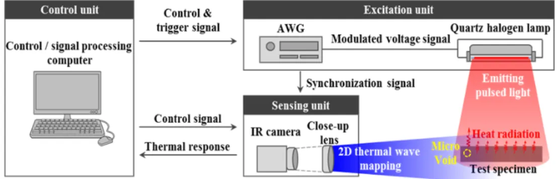
Fig. 1 shows an overall schematic of the active infrared thermography system composed of excitation, sensing, and control units. The excitation unit consists of an arbitrary wave generator (AWG) and a quartz halogen lamp. AWG generates a modulated voltage signal according to a control signal sent by the control unit. The quartz halogen lamp used in this system has a wavelength range of 0.4 μm to 1.2 μm (near infrared) and a maximum peak power of 1.5 kW. Note that the quartz halogen lamp which has the wavelength range of near infrared is useful for penetrating much deeper into a specimen because shorter wavelengths are likely to lead to more efficient thermal wave generation in the thickness direction [12]. The sensing unit is comprised of an infrared camera with a close-up lens. The infrared camera with an uncooled micro bolometer detector is used to capture 2D raw thermal images of the radiated heats from the EMC surface. The infrared camera has a thermal time constant of 7 ms, a noise equivalent temperature difference of 30 mK,
640 × 480 pixels, a maximum sampling rate of 50 Hz, and a spectral range of 7.5 to 14 μm. The close-up lens has a focal length of 30 mm and a stand-off distance of 50 mm. This lens is additionally employed to enhance the spatial resolution up to 30 μm/pixel. The data acquisition and processing are controlled by LABVIEW® and MATLAB® programs installed in the control unit, respectively.
The working principle of the active infrared thermography system is as follows. First, the control unit sends out a control and trigger signal to the excitation and sensing units. AWG in the excitation unit sends out a pulse modulated voltage signal to the quartz halogen lamp, and the corresponding pulsed light is emitted from the quartz halogen lamp to the test specimen. Simultaneously, AWG sends a synchronization signal to the infrared camera, and the infrared camera integrated with a close-up lens measures the heat radiation from the surface of the test specimen. When the test specimen is thermally stimulated by the quartz halogen lamp, the surface temperature of the sample increases. As the heat energy diffuses toward the thickness direction of the specimen, the heat diffusion rate is reduced and the temperature rises locally at the void [13].
2.2. Description of Experimental Setup
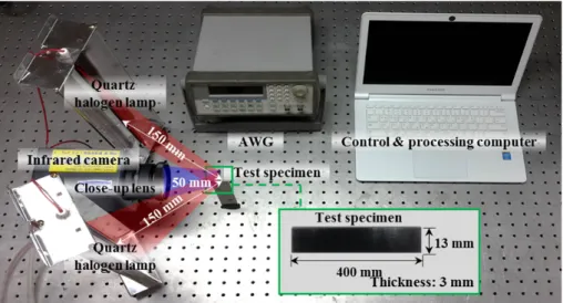
Fig. 2 shows an experimental setup of the active infrared thermography system and an EMC specimen. AWG (33220A, Agilent) generates a pulse heating of 3 sec and a cooling of 17 sec. Two quartz halogen lamps, which are 15 cm apart from the test specimen, emit the pulse light modulated by AWG. The power level of each quartz halogen lamp is 1.5 kW, and this power intensity increases the surface temperature of the EMC from the room temperature up to 33.61°C. Note that this level of temperature increase does not damage the test specimen. The corresponding thermal responses are measured in the time domain using the infrared camera (VarioCam®hr, InfraTec) synchronized with AWG. The infrared camera is 50 mm apart from the test specimen, and acquires raw thermal images with a sampling rate of 50 Hz. Once the thermal responses are measured, the data is transmitted to the control computer and processed by the proposed baseline-free subsurface micro void visualization algorithm described in the following section.
3. Development of Baseline-free Subsurface Micro Void Visualization Algorithm
This section explains how subsurface micro voids are detected and visualized using the raw thermal images measured only from the current test condition of the test specimen without relying on the baseline data obtained from its intact condition. When a pulse light is illuminated onto the surface of the intact specimen, the local heat flux in an isotropic and homogeneous medium in one-dimensional space can be expressed by the following Fourier’s equation [14]:
(1)
where is the local heat flux in the thickness direction, and is the thermal conductivity. Because of the homogeneity of the EMC specimen, the heat flux in the thickness direction would be uniform over the surface. However, the heat flux depends on the thermal conductivity of the material, and the presence of the subsurface micro void can alter the thermal conductivity. This phenomenon can further be scrutinized using Fourier’s law for a homo- geneous material of one-dimensional geometry:
∆ ∆ ∆ ∆ (2)
where ΔQ/Δt is the amount of heat transferred by incident light, A is the surface area and ΔT is the temperature difference. Because ΔQ/Δt and A are constant, ΔT should decrease as k increases. Accordingly, the surface temperature profile above the subsurface micro void will be different from that of the surrounding area. For example, if a void is formed in a fiber reinforced epoxy, the thermal conductivity of fiber reinforced epoxy (0.2 W/m·K) is eight times bigger than that of air (0.025 mm2/s). Therefore, the surface temperature above the subsurface void is much higher compared to that of the surrounding area. This temperature variation over the surface is reflected in the measured raw thermal images. The raw thermal images are processed by the proposed baseline-free subsurface micro void visualization algorithm to extract and isolate void-induced perturbation. Such baseline-free diagnostic is able to provide instantaneous diagnosis and minimize false alarms caused by irregular surface conditions of the test specimen and arbitrary noise components of the raw thermal images, making it suitable for online inspection.
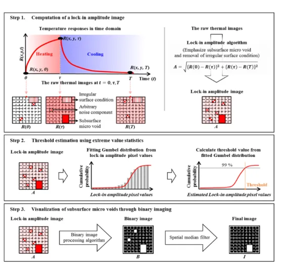
Fig. 3 shows the overall schematic of the proposed baseline-free subsurface micro void visualization algorithm. The algorithm consists of three major steps: (1) computation of a
lock-in amplitude image using 3-bucket method, (2) threshold estimation using extreme value statistics, and (3) visualization of the subsurface micro void through binary imaging. Detailed procedures are described below.
Step 1. Computation of a Lock-In Amplitude Image
The proposed subsurface micro void visuali- zation algorithm starts with the computation of a lock-in amplitude image. Based on the preliminary study using the EMC specimens, the amplitude image shows that the void area has much more signal difference compared with the intact area, rather than the phase image. Note that, the external noise affected by environmental reflections, non-uniform heating,
emissivity variations and area geometry is well eliminated on the phase image than the amplitude image, the amplitude image can distinguish the damage area from the intact area without the noise component from the further image processing algorithms in Step 2 of the article. Once the raw thermal images are recorded by the infrared camera in the time domain, the lock-in amplitude image is constructed by calculating the following lock-in amplitude values for all pixel points [15]:
(2)
where R(x, y, t) is the raw thermal response at a spatial point (x, y) and a time point t. τ is the
duration of the pulse heating, and T is the total time of heating and cooling cycle. A(x, y) denotes the processed lock-in amplitude. Equation (2) extracts the thermal gradient synchronized only with the excitation halogen lamp, and other heat sources, which are not synchronized with the excitation halogen lamp, do not affect A(x,
y). Therefore, the lock-in amplitude image
removes uneven heating and surface reflection caused by the irregular surface condition.
Step 2. Threshold Estimation Using Extreme Value Statistics
The binary imaging in the next step is based on the premise that the surface temperature around the subsurface micro void rises higher than the rest of the area. To visualize the void locations where the temperature exceeds a certain value, a threshold for such classification is determined in this step using extreme value statistics. The extreme value statistics is a branch of statistics that models the statistical properties of extreme values in either the upper or lower tails of sampled data [16]. Among available extreme value distributions, a Gumbel distribution is selected in this study to characterize the upper tail distribution of the processed lock-in amplitude values based on goodness-of-fit analysis. Once the best-fit Gumbel distribution is estimated, the threshold value corresponding to a one-sided 99% confidence interval is determined.
Step 3. Visualization of Subsurface Micro Voids Through Binary Imaging
In this step, binary imaging is used to visualize the surface areas affected by subsurface micro voids. That is, the values of the pixel points, where the corresponding lock-in amplitude values exceed the predetermined threshold value, are set to one, and the rest to zero:
(3)
Next, by applying a spatial median filter [17], remaining sparse noise components are removed and subsurface micro voids are visualized.
4. Experimental investigation
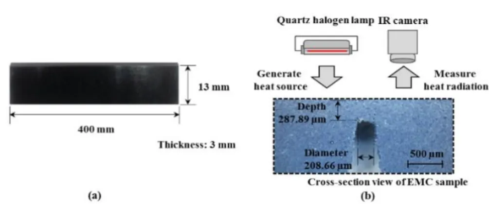
In this section, the proposed active infrared thermography system and void visualization algorithm are used to detect subsurface micro voids in the EMC specimens provided by Samsung Electronics Co., Ltd. Each EMC specimen has dimensions of 400 mm × 13 mm × 3 mm. Using a laser drilling machine, subsurface micro voids with varying diameters (150 µm ~ 300 µm) and depths from the inspected (top) surface (150 µm ~ 300 µm) are introduced to the EMC specimens as shown in Figs. 4 (a) and (b). Total 36 EMC specimens are tested and labeled as EMC 1 to EMC 36. EMC 1 to EMC 18 have subsurface micro voids, and EMC 19 to EMC 36 are intact. Note that the details of the material compounds and design parameters are unknown to the authors due to the confidentiality of the EMC specimens.
The active infrared thermography system activates two quartz halogen lamps with a 3 sec pulse input, and the infrared camera synchronized with the lamps measures heat emission form the surface of EMC for 20 sec. Figs. 5 (a), (b) and (c) show the representative raw thermal images measured at 0 sec, 3 sec, and 20 sec, respec- tively, which are used for calculating the lock-in amplitudes. In the raw thermal image taken at 3 sec, higher temperature increase is observed near the subsurface void.
Once raw thermal images are obtained, the lock-in amplitude image is constructed using Equation 2. Comparison of Fig. 5(b) and Fig. 6 (a) reveals that uneven heating and surface reflection caused by the irregular surface
Fig. 4 Descriptions of a representative EMC test specimen (EMC 1): (a) a top view of the EMC specimen and (b) a cross-section view of the EMC specimen with a subsurface micro void
Fig. 5 The representative raw thermal images obtained from EMC 1 at (a) 0 sec, (b) 3 sec and (c) 20 sec
Fig. 6 Visualization of the subsurface micro void in EMC 1: (a) a lock-in amplitude image and (b) a binary image
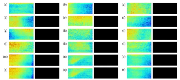
Fig. 7 The lock-in amplitude and binary images obtained from EMCs with subsurface micro voids: Subfigures (a) to (r) show the test results from EMC 1 to EMC 18, respectively)
condition are removed in the processed lock-in amplitude image. Next, the binary image is constructed in Fig. 6(b) to demonstrate that unwanted noises are removed and the subsurface micro void is successfully visualized. Figs. 7 and 8 show the test results from all 36 EMC specimens (Fig. 7 for EMCs 1 to 18 with defects, and Fig. 8 for intact EMCs 19 to 36). Subsurface micro voids are successfully visualized in all 36 specimens without any false alarms. The whole computation time of the baseline-free subsurface micro void visualization algorithm per one EMC sample is less than 1 second with MATLAB® program run on the 3.60 GHz processor (Intel® CoreTM, i7-4790).
5. Conclusion
In this study, the active infrared thermography system with a baseline-free defect detection algorithm is developed to automatically and instantaneously detect and visualize subsurface (below 150 µm ~ 300 µm from the inspection surface) micro (150 µm ~ 300 µm in diameter) voids in epoxy molding compounds (EMCs) used in electronic chip packaging. Experimental tests are performed using laboratory-scale EMC
specimens. The proposed active infrared thermography system and defect visualization algorithm offer the following advantages for EMC specimen inspection: (1) fully noncontact, nondestructive, and nonintrusive inspection, and (2) automated, instantaneous and reference-free inspection suitable for online applications. However, further investigations are warranted before the proposed active infrared thermography system can be applied during real manufacturing processes of electronic devices. First, the use of a flash lamp instead of a quartz halogen lamp is under investigation to reduce the data collection time thanks to its high intensity light emission within several mille seconds. Second, the EMC components used in electronic devices have intricate geometries, and their complexities are not considered in this study.
Acknowledgment
This work was supported by the Korea Ministry of Land, Infrastructure and Transport (MOLIT) as U-City Master and Doctor Course Grant Program and Manufacturing Core Technology Team in Global Technology Center of Samsung Electronics Co., Ltd.
Fig. 8 The lock-in amplitude and binary images obtained from EMCs without any subsurface micro voids: Subfigures (a) to (r) show the test results from EMC 19 to EMC 36, respectively
References
[1] H. Xiao, "Introduction to Semiconductor Manufacturing Technology," Washington: SPIE press in United States, (2012) [2] M. K. Abdullah, M. Z. Abdullah, M. A.
Mujeebu and S. K. Kamaruddin, "A study on the effect of epoxy molding compound (EMC) rheology during encapsulation of stacked-CHIP scale packages (S-CSP),"
Journal of Reinforced Plastics and Composites, Vol. 28, pp. 2527-2538 (2009)
[3] A. Haleh, "Hygroscopic swelling and sorption characteristics of epoxy molding compounds used in electronic packaging,"
IEEE Transactions on Components and Packaging Technologies, Vol. 26, pp. 206-
214 (2003)
[4] C. Y. Khor, M. A. Abdullah, Z. M. Ariff and W. C. Leong, "Effect of stacking chips and inlet positions on void formation in the encapsulation of 3D stacked flip- chip package," International Communications
in Heat and Mass Transfer, Vol. 39,
pp. 670-680 (2012)
[5] T. Tian, K. Chen, A. MacDowell, D. Parkinson, T. Lai and K. N. Tu, "Quantitative X-ray microtomography study of 3-D void growth induced by electro- migration in eutectic SnPb flip-chip solder joints," Scripta Materialia, Vol. 65, pp. 646-649 (2011)
[6] M. Clark, S. Sharples and M. Somekh, "Non-contact acoustic microscopy," Meas-
urement Science and Technology, Vol. 11,
pp. 1792-1801 (2000)
[7] C. Meola and M. Carlomagno, "Recent advances in the use of infrared thermo- graphy," Measurement Science and Tech-
nology, Vol. 15, R27-R58 (2004)
[8] G. Busse, D. We and W. Karpen, "Thermal wave imaging with phase sensitive modulated thermography," Journal
of Applied Physics, Vol. 71, No. 8, pp.
3962-3965 (1992)
[9] W. Bai and B. S. Wong, "Evaluation of defects in composite plates under convective environments using lock-in thermography,"
Measurement Science and Technology, Vol.
12, pp. 142-150 (2001)
[10] M. Choi, K. Kang, J. Park, W. Kim and K. Kim, "Quantitative determination of a subsurface defect of reference specimen by lock-in infrared thermography," NDT&E
International, Vol. 41, pp. 119-124 (2008)
[11] S. Dudzik, "Approximation of thermal background applied to defect detection using the methods of active thermography,"
Metrology and Measurement Systems, Vol.
17, pp. 621-636 (2010)
[12] M. Balu, T. Baldacchini, J. Carter, T. B. Krasieva, R. Zadoyan and B. J. Tromberg, "Effect of excitation wavelength on penetration depth in nonlinear optical microscopy of turbid media," Journal of
Biomedical Optics, Vol. 14, 010508 (2009)
[13] G. Traxler, M. Scheerer and C. Steiger, "Square pulse thermography system design considerations for detection of voids inside of the material with different properties and finite differences," Proceedings of
SPIE, Vol. 5679, pp. 118-128 (2005)
[14] HL. John IV, HL. John V, "A heat transfer textbook," 4th ed. Cambridge: Phlogiston Press in United States, (2008) [15] J. Liu, W. Yang and J. Dai, "Research on
thermal wave processing of lock-in thermography based on analyzing image sequences for NDT," Infrared Physics &
Technology, Vol. 53, pp. 348-357 (2010)
[16] A. Rinaldi and D. Krajcinovic, "Statistical damage mechanics and extreme value theory," International Journal of Damage
Mechanics, Vol. 16, pp. 57-76 (2015)
[17] R. H. Chan, C. W. Ho, Nikolova M, "Salt-and-pepper noise removal by median- type noise detectors and detail-preserving regularization," IEEE Transaction on Image Processing, pp. 14 1479-1485 (2005)