Extracting optical modes of organic
light-emitting diodes using quasi-periodic WO
3
nanoislands
Jin Yeong Kim, Chung Sock Choi, Woo Hyun Kim, Dong Young Kim, Do Hong Kim, and Kyung Cheol Choi*
Department of Electrical Engineering, KAIST, Daejeon 305-701, Korea
Abstract: Quasi-periodic WO3 nanoislands are introduced to extract two
optical modes in organic light-emitting diodes. The nano-scaled and size-tunable WO3 islands were fabricated by use of wet-etching with
self-aggregated Ag mask. The improvement of light extraction efficiency originates to the recovery of light losses which are surface plasmon mode and waveguide mode. As a result, external quantum efficiency and power efficiency were increased. No changes in emission spectrum and CIE color coordinates with WO3 nanoislands at various observation angles are
desirable if this device is to be utilized in optical system. Furthermore, cost-effective fabrication makes it possible to adopt this system in large area fabrication.
©2013 Optical Society of America
OCIS codes: (230.3670) Light-emitting diodes; (240.6680) Surface plasmons; (230.7370)
Waveguides; (220.4241) Nanostructure fabrication. References and links
1. R. Meerheim, M. Furno, S. Hofmann, B. Lüssem, and K. Leo, “Quantification of energy loss mechanisms in organic light-emitting diodes,” Appl. Phys. Lett. 97(25), 253305 (2010).
2. P. A. Hobson, J. A. E. Wasey, I. Sage, and W. L. Barnes, “The role of surface plasmons in organic light-emitting diodes,” IEEE J. Sel. Top. Quantum Electron. 8(2), 378–386 (2002).
3. J. Y. Kim and K. C. Choi, “Improvement in outcoupling efficiency and image blur of organic light-emitting diodes by using imprinted microlens arrays,” J. Disp. Technol. 7(7), 377–381 (2011).
4. B. Riedel, Y. Shen, J. Hauss, M. Aichholz, X. Tang, U. Lemmer, and M. Gerken, “Tailored highly transparent composite hole-injection layer consisting of Pedot:PSS and SiO2 nanoparticles for efficient polymer
light-emitting diodes,” Adv. Mater. 23(6), 740–745 (2011).
5. C. S. Choi, S.-M. Lee, M. S. Lim, K. C. Choi, D. Kim, D. Y. Jeon, Y. Yang, and O. O. Park, “Improved light extraction efficiency in organic light emitting diodes with a perforated WO3 hole injection layer fabricated by
use of colloidal lithography,” Opt. Express 20(Suppl 2), A309–A317 (2012).
6. Y.-C. Kim, S.-H. Cho, Y.-W. Song, Y.-J. Lee, Y.-H. Lee, and Y. R. Do, “Planarized SiNx/spin-on-glass photonic crystal organic light-emitting diodes,” Appl. Phys. Lett. 89(17), 173502 (2006).
7. S. Jeon, J.-W. Kang, H.-D. Park, J.-J. Kim, J. R. Youn, J. Shim, J. Jeong, D.-G. Choi, K.-D. Kim, A. O. Altun, S.-H. Kim, and Y.-H. Lee, “Ultraviolet nanoimprinted polymer nanostructure for organic light emitting diode application,” Appl. Phys. Lett. 92(22), 223307 (2008).
8. Y. Sun and S. R. Forrest, “Enhanced light out-coupling of organic light-emitting devices using embedded low-index grids,” Nat. Photonics 2(8), 483–487 (2008).
9. K. Sieradzki, K. Bailey, and T. L. Alford, “Agglomeration and percolation conductivity,” Appl. Phys. Lett.
79(21), 3401–3403 (2001).
10. J. H. Son, Y. H. Song, H. K. Yu, and J.-L. Lee, “Effects of Ni cladding layers on suppression of Ag agglomeration in Ag based ohmic contacts on p-GaN,” Appl. Phys. Lett. 95(6), 062108 (2009).
11. S. K. Sharma and J. Spitz, “Hillock formation hole growth and agglomeration in thin silver films,” Thin Solid Films 65(3), 339–350 (1980).
12. B. Munro, S. Kramet, P. Zapp, and H. Krug, “Characterization of electrochromic WO3-layers prepared by sol-gel
nanotechnology,” J. Sol-Gel Sci. Techn. 13, 673–678 (1998).
13. R. Armitage, M. Cich, M. Rubin, and E. R. Weber, “A method to pattern Pd over-layers on GdMg films and its application to increase the transmittance of metal hydride optical switches,” Appl. Phys. A:Mater 71(6), 647–650 (2000).
14. A. O. Altun, S. Jeon, J. Shim, J.-H. Jeong, D.-G. Choi, K.-D. Kim, J.-H. Choi, S.-W. Lee, E.-S. Lee, H.-D. Park, J. R. Youn, J.-J. Kim, Y.-H. Lee, and J.-W. Kang, “Corrugated organic light emitting diodes for enhanced light extraction,” Org. Electron. 11(5), 711–716 (2010).
15. W. H. Koo, S. Y. Boo, S. M. Jeong, S. Nishimura, F. Araoka, K. Ishikawa, T. Toyooka, and H. Takezoe, “Controlling bucking structure by UV/ozone treatment for light extraction from organic light emitting diodes,” Org. Electron. 12(7), 1177–1183 (2011).
16. W. H. Koo, S. M. Jeong, S. Nishimura, F. Araoka, K. Ishikawa, T. Toyooka, and H. Takezoe, “Polarization conversion in surface-plasmon-coupled emission from organic light-emitting diodes using spontaneously formed buckles,” Adv. Mater. 23(8), 1003–1007 (2011).
17. S. J. Fang, S. Haplepete, W. Chen, C. R. Helms, and H. Edwards, “Analyzing atomic force microscopy images using spectral methods,” J. Appl. Phys. 82(12), 5891–5898 (1997).
18. W. Ma, C. Yang, and A. J. Heeger, “Spatial fourier-transform analysis of the morphology of bulk heterojunction materials used in “plastic” solar cells,” Adv. Mater. 19(10), 1387–1390 (2007).
19. Y. R. Do, Y.-C. Kim, Y.-W. Song, and Y.-H. Lee, “Enhanced light extraction efficiency from organic light emitting diodes by insertion of a two-dimensional photonic crystal structure,” J. Appl. Phys. 96(12), 7629 (2004).
20. W. H. Koo, S. M. Jeong, F. Araoka, K. Ishikawa, S. Nishimura, T. Toyooka, and H. Takezoe, “Light extraction from organic light-emitting diodes enhanced by spontaneously formed buckles,” Nat. Photonics 4(4), 222–226 (2010).
21. J. Meyer, S. Hamwi, T. Bülow, H.-H. Johannes, T. Riedl, and W. Kowalsky, “Highly efficient simplified organic light emitting diodes,” Appl. Phys. Lett. 91(11), 113506 (2007).
22. J. Li, M. Yahiro, K. Ishida, H. Yamada, and K. Matsushige, “Enhanced performance of organic light emitting device by insertion of conducting/insulating WO3 anodic buffer layer,” Synth. Met. 151(2), 141–146 (2005).
23. Y. Bai, J. Feng, Y.-F. Liu, J.-F. Song, J. Simonen, Y. Jin, Q.-D. Chen, J. Zi, and H.-B. Sun, “Outcoupling of trapped optical modes in organic light-emitting devices with one-step fabricated periodic corrugation by laser ablation,” Org. Electron. 12(11), 1927–1935 (2011).
24. K. Ishihara, M. Fujita, I. Matsubara, T. Asano, S. Noda, H. Ohata, A. Hirasawa, H. Nakada, and N. Shimoji, “Organic light-emitting diodes with photonic crystals on glass substrate fabricated by nanoimprint lithography,” Appl. Phys. Lett. 90(11), 111114 (2007).
25. J. Hauss, T. Bocksrocker, B. Riedel, U. Lemmer, and M. Gerken, “On the interplay of waveguide modes and leaky modes in corrugated OLEDs,” Opt. Express 19(S4), A851–A858 (2011).
26. Y.-J. Lee, S.-H. Kim, J. Huh, G.-H. Kim, Y.-H. Lee, S.-H. Cho, Y.-C. Kim, and Y. R. Do, “A high-extraction-efficiency nanopatterned organic light-emitting diode,” Appl. Phys. Lett. 82(21), 3779–3781 (2003). 1. Introduction
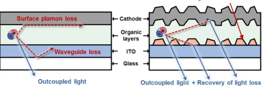
Organic Light Emitting Diodes (OLEDs) have attracted great interest due to their potential applications in, for example, display devices and lighting systems. While the achievement of highly efficient OLEDs is important for utilization in various applications, one of the problems of OLEDs is their low out-coupling efficiency due to various optical loss channels in the device [1]. One of loss channels is the substrate mode, which is induced by differences in the refractive index between the layers [2]. To address this problem, a micro-lens array and a scattering layer have been reported [3, 4]. A large portion of the light loss also occurs from the surface plasmon polaritons (SPPs) and from the waveguide mode. A surface plasmon is a type of charge oscillation along the surface of the metal; the light loss induced by the surface plasmon mode is strongly confined between the organic layers and the metal cathode [5]. The waveguide mode is trapped in the thick transparent conductive oxide (TCO) layer, which has a higher refractive index than the adjacent layers. Various techniques have been reported to extract two optical modes to improve light efficiency; these techniques include use of photonic crystals and nanostructures with periodic patterns [6–8].
A nano-scaled periodic structure is a good candidate to extract the light loss at a specific emission wavelength; however, fabrication to achieve nano-scaled periodic structures, for example, photolithography and E-beam lithography, are complex and non-economical. Moreover, unexpected changes of color coordinate and electrical property induced by the nanostructure are undesirable if such a device is to be utilized in an optical system or a display device.
For this paper, we introduced quasi-periodic Tungsten trioxide (WO3) nanoislands to
extract the waveguide mode and the surface plasmon mode which are trapped in OLEDs. Two optical modes can be extracted through Bragg scattering by inserting a grating structure with a periodicity of several hundred nanometers, as shown in Fig. 1. A self-aggregated silver (Ag) layer, which is achieved using only a thermal annealing process, was used as mask for WO3 wet-etching. The suggested method, based on wet-etching, is extremely simple and
size-tunable. No angular dependency of emission property in this study is desirable if we are to adopt such a device for various optical applications. Furthermore, cost-effective fabrication
without photolithography makes it possible to adopt WO3 nanoislands in large area
fabrication.
Fig. 1. Schematic cross section of devices (left) without and (right) with quasi-periodic WO3
nanoislands considered in this work. 2. Experimental methods
We fabricated quasi-periodic nanoislands using the wet-etching process, as shown in Fig. 2. WO3 was chosen as the nanoislands due to its good charge injection property [5]. Glass
substrates coated with 150 nm thick indium tin oxide (ITO) were cleaned using isopropyl alcohol and DI water in an ultrasonic bath. On a prepared clean ITO glass (2.5 cm × 2.5 cm), 30 nm WO3 and 20 nm Ag were sequentially deposited by means of thermal evaporation (Fig.
2(a)). After this deposition, the sample was heated to 300 °C for 30 min in an N2 environment
to achieve the self-aggregated mask (Fig. 2(b)). In the literature, Ag has been shown to aggregate by itself at high temperature [9, 10]; the size of an aggregated Ag layer can be tuned using the Ag thickness, annealing temperature, annealing time, and substrate morphology [11]. The amount of aggregation increases as the annealing temperature and time increase before reaching the saturation point, so we heated the sample to a high temperature, sufficient to allow the Ag nanoislands to aggregate by themselves [9]. After that, the WO3
layer was dipped in 1 mM Potassium hydroxide (KOH) solution for 90s at room temperature to selectively etch the WO3 (Fig. 2(c)) [12, 13]. The Ag mask was removed using a nitric and
sulfuric acid mixture (MA-S02, Dongwoo Fine-Chem) for 90s at room temperature.
Fig. 2. Fabrication procedures of WO3 nanoislands: (a) Depostion of WO3, Ag on ITO glass,
(b) thermally annealing process to achieve self-aggregated Ag, (c) WO3 wet-etching with
self-aggregated Ag mask.
To evaluate the effect of the WO3 nanoislands on the electroluminescence, a OLED
device with 50 nm N,N'-bis(naphthalen-1-yl)-N,N'-bis(phenyl)-benzidine (NPB) hole transport layer / 50 nm tris(8-quinolinolato) aluminum (Alq3) emitting layer / 1 nm lithium
fluoride (LiF) electron injection layer / 100 nm aluminum (Al) metallic cathode, was fabricated by thermal evaporation. The devices were encapsulated with UV curable resin in a nitrogen environment. A Keithley 2400 sourcemeter was used to measure the current density and voltage. The luminance and emission spectrum were measured using a spectroradiometer (CS-2000, Konica Minolta) at various observation angles. Emissions were measured with various emission angles (θ) ranging from 0° to 60° with an increment of 10°; the azimuthal angle (φ) was changed from 0° to 360° with an increment of 15° [14–16]. The emission spectra at all emission and azimuthal angles are interpolated to calculate the power efficiency
and external quantum efficiency. An optical calculation was performed using commercial MATLAB software (MathWorks, Inc.) based on the transfer matrix method.
3. Results and discussion
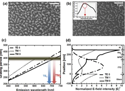
Figure 3 shows SEM images of (a) the self-aggregated Ag mask that is achieved by only thermal annealing and (b) WO3 nanoislands after wet-etching with the Ag mask. As can be
seen in the SEM images, WO3 nanoislands were well fabricated by selectively wet-etching. It
is difficult to obtain periodicity of nanoislands from SEM images. Thus, the power spectrum in frequency domain was calculated using following equation [17, 18],
2 0 0 ( , ) 1 exp( 2 ) exp( 2 ) ( , ) L L x y x y PS f f i xf i yf I x y dxdy L π π =
− − (1)where L is the image size, fx and f are the spatial frequencies along the x-axis and y-axis, y
respectively. I is the contrast intensity of SEM image. In this experiment, WO3 nanoislands
have no directionality in spatial domain. Thus, power spectrum as a function of radial frequency can be achieved by averaging over polar angles using following equation [17, 18],
2 0 ( ) 1 ( , ) 2 PS f PS f d π θ θ π =
(2)where f is radial frequency, θ is polar angle. Figure 3(b) (inset) shows the calculated power spectrum of WO3 nanoislands versus the wavelength instead of the radial frequency. Power
spectrum shows the broad spectrum around 400 nm, thus, we used the peak periodicity for calculating Bragg scattering condition, to allow for simple calculation.
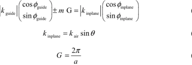
To determine the effect of nanoislands on extracting optical modes in OLEDs, we calculated the dispersion relation and the electric field profile of various modes in the OLEDs. We assumed that the thickness of the glass and the cathode are infinite, and those of ITO, NPB, and Alq3 are 150 nm, 50 nm, and 50 nm, respectively. The refractive indices of
glass and NPB are fixed at 1.53 and 1.79, respectively [19]. For the refractive indices of ITO, Alq3, and aluminum (Al), a function of the wavelength was used [1]. The large portion of
light losses, which are trapped in the form of waveguide mode and surface plasmon mode, can be recovered by nanoislands if the periodicity of nanoislands satisfies the Bragg scattering condition [5]. The Bragg scattering condition can be calculated using the following equation, guide inplane guide inplane guide inplane cos cos G sin sin k φ m k φ φ φ ± = (3)
inplane airsin
k =k θ (4) 2 G a π = (5)
where kair is the wave vector of the free space light, θ is the emission angle, kinplane is the inplane component of kair , kguide is the wave vector of the waveguide mode, φ is the azimuthal angle of the propagation of light, a is peak periodicity of nanoislands, and m is an integer. The power spectrum of quasi-periodic nanoislands is broad in the frequency domain, but we assumed peak wavelength of the power spectrum as a peak periodicity of quasi-periodic nanoislands, a = 400 nm [20]. The grating vector G can be considered as having 1-dimension because the nanoislands have no directionality in spatial domatin [20]. For the
isotropic nanostructure like in this study, the Bragg scattering condition in normal direction can be simplified using the following equation,
guide 2 0 k m a π ± = (6)
Figure 3(c) shows the calculated periodicity of nanoislands as function of emission wavelength in normal direction to extract two optical modes of OLEDs. When the peak periodicity of quasi-periodic WO3 nanoislands is about 400 nm, which is represented as the
horizontal line Fig. 2(c), the matching condition occurs at 600 nm for the TM1 mode, 680 nm
for the TE0 mode, and 720 nm for the TM0 mode.
Figure 3(d) shows the electric field profile for the TE and TM modes in the OLED device at 530 nm, which is the peak frequency of Alq3. Two light loss channels, the waveguide mode
and the surface plasmon mode, are highly confined in the form of the TE0 mode and the TM0
mode, respectively. According to optical calculation, as shown in Fig. 3(c) and Fig. 3(d), extraction of two optical modes at 700 nm emission wavelength is expected through Bragg scattering, given the peak periodicity of nanoislands, 400 nm.
Fig. 3. SEM images of the (a) Ag mask: self-aggregated Ag on 30 nm WO3 after thermal
annealing process (b) quasi-periodic WO3 nanoislands after wet-etching. Inset figure is power
spectrum as function of periodicity instead of wavenumber. The power spectrum was calculated using the SEM image; a 400 nm peak periodicity was achieved. (c) Calculated isotropic grating period as function of emission wavelength to extract waveguide mode and surface plasmon mode. Horizontal line represents a peak periodicity of 400 nm, which is achieved by the power spectrum in this experiment. (d) Normalized electric field profiles of TE0 and, TM0 modes in OLEDs at 530 nm, which is the Alq3 emission.
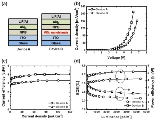
The device characteristics were measured as shown in Fig. 4. The measurements were performed varying emission angles (θ) from 0° to 60°, while the azimuthal angle (φ) was
fixed, because the quasi-periodic nanoislands has no angular dependency on the azimuthal angle [20]; the details will be discussed later. The current density-voltage characteristics of the devices are shown in Fig. 4(b). Operating voltage was reduced by insertion of WO3 which
has good hole injection property [21, 22]. Current efficiency, as shown in Fig. 4(c), is 2.99 cd/A at 10 mA/cm2 and 3.32 cd/A at 100 mA/cm2 without nanoislands; current efficiency was
3.66 cd/A at 10 mA/cm2 and 4.03 cd/A at 100 mA/cm2 with WO
3 nanoislands. Figure 4(d)
shows the EQE-luminance measurement results. EQE was 0.98% at 1000 cd/m2 without WO 3
nanoislands, and 1.22% with WO3 nanoislands. Power efficiency was increased by 42% at
Fig. 4. (a) Schematic of devices in this experiment (b) Current density (J)-voltage (V), (c) The current efficiency versus current density, and (d) (solid line) the EQE and (dotted line) the power efficiency versus luminance characteristics in this experiment.
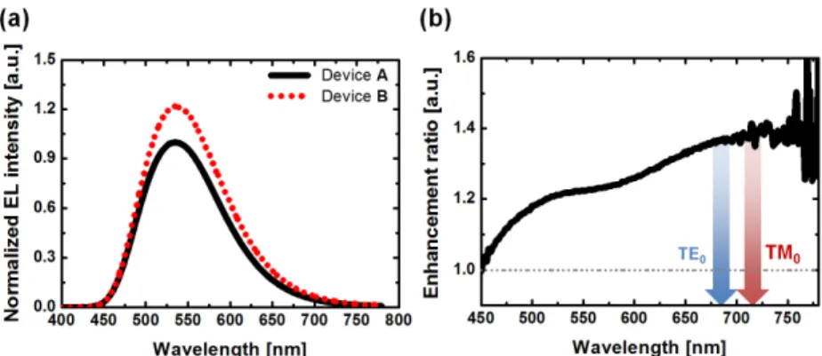
Figure 5(a) shows measured emission spectra of the OLED in the normal direction to verify the extraction of two optical modes by nanoislands. The radiant intensity was enhanced over a wide wavelength region, thus, we calculated the enhancement ratio of measured EL spectra in order to verify the wavelength dependency, as shown in Fig. 5(b). There is a peak value of enhancement ratio around 700 nm emission wavelength. In the previous part, we calculated the Bragg scattering matching condition given a peak periodicity of WO3
nanoislands which is around 400 nm; the resulting values are 670 nm for the TE0 mode
(waveguide mode) and 720 nm for the TM0 mode (surface plasmon mode). As calculated
from the Bragg condition, as shown in Fig. 3(c), the broad enhancement of the radiant intensity originated from the extraction of the optical modes with an emission wavelength of around 700 nm. For a periodic nanostructure, each mode has one certain Bragg scattering condition; thus, TE and TM mode extraction can be shown at a specific wavelength [23, 24]. However, the Bragg scattering condition for an asymmetric nanostructure in this study has a broad matching wavelength instead of a certain wavelength. Therefore, extraction of the TE0
mode and the TM0 mode shows a broad spectrum around 670 nm and 720 nm, respectively.
The use of a polarizer is one way to distinguish each mode [25], but a high-order term which influences the surface plasmon loss and the waveguide loss is also measured in this case. It is difficult to determine the exact portion of channels of the extracted light.
Fig. 5. (a) The measured EL spectra at 20 mA/cm2 of the fabricated OLED (solid line) without
and (dotted line) with quasi-periodic WO3 nanoislands (b) Enhancement ratio of EL spectra
with WO3 nanoislands as function of wavelength.
Figure 6 shows the current-voltage characteristics of the hole-only devices. We also fabricated a device with 30 nm of WO3 film. It was noted that hole injection of the device
with the WO3 film is improved compared to a device without WO3 film [5]. The current
characteristic of the hole-only device with WO3 nanoislands is also improved compared to a
control device. Thus, we conclude that more hole injection by WO3, which is generally used
as a hole injection material, contributes to reducing the operating voltage. In other words, the power efficiency of OLEDs with WO3 nano-islands is improved as follows: 1) the light losses
that occur in the forms of the waveguide mode and the surface plasmon mode are extracted by Bragg scattering, and 2) the operating voltage is reduced by WO3 due to its hole injection
characteristics.
Fig. 6. I-V characteristics of the hole-only with ITO/hole injection layer/NPB (150 nm)/ Al (100 nm) [0 nm WO3 (circle), 30 nm WO3 film (square), 30 nm WO3 nanoislands (triangle)]
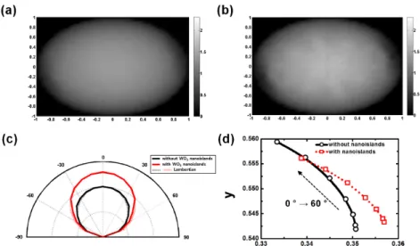
Figure 7 shows the radiant intensity profiles for all observation angles (θ, φ) (a) without and (b) with WO3 nanoislands. There was no dependency at all observation angles when the
nanoislands were inserted in the OLED device. A periodic nanostructure is a good candidate for more light extraction at specific emission wavelengths but the symmetric geometry of nanostructure induces a specific emission pattern [16]. The WO3 nanoislands, proposed in this
study, induce no specific angular dependency due to the broad range of grating vectors in the azimuthal directions [23]. Figure 7(c) shows the radiant intensity for the emission angle (θ) while the azimuthal angle (φ) is fixed; the proposed WO3 nanoislands extracts more lights
while the Lambertian emission is maintained. The CIE color coordinates are almost unchanged, as shown in Fig. 7(d). When the emission angle was increased from 0° to 60°, the CIE coordinates were changed from (0.35, 0.54) to (0.33, 0.56) for the OLED without WO3
nanoislands, and from (0.36,0.54) to (0.34,0.56) for the OLED with WO3 nanoislands.
Changes of the CIE coordinates of both devices are nearly identical at 6% and 5% for the x and y coordinates, respectively.
Fig. 7. The measured radiant intensity profiles at various observation angles (a) without and (b) with WO3 nanoislands (c) Angular dependency of light intensity for devices (black line)
without and (red line) with WO3 nanoislands while azimuthal angle is fixed. Radiation profile
of a Lambertian emission (dotted line) for each device is also represented. (d) CIE color coordinate change for the emission angle of devices (solid line) without and (dotted line) with WO3 nanoislands.
4. Conclusions
In summary, a nano-scaled and quasi-periodic WO3 islands were fabricated to extract optical
modes in OLED device. The fabrication method, based on wet-etching, is extremely simple and size-tunable. The light losses, which are trapped in terms of the surface plasmon mode (TM0) and the waveguide mode (TE0), were recovered by Bragg scattering. Operating voltage
is also reduced due to the good charge injection of the WO3. Invariance of emission spectrum
and CIE color coordinates at various observation angles is desirable if this device is to be utilized in an optical system or display device. Furthermore, cost-effective fabrication without photolithography makes it possible to adopt in large area fabrication.
Acknowledgments
This research was supported by Basic Science Research Program through the National Research Foundation of Korea (NRF) funded by the Ministry of Education, Science and Technology (CAFDC-20100009890). This work was supported by the Industrial Strategic Technology Development Program, (No. 10035573), funded by the Ministry of Knowledge Economy (MKE, Korea). The authors also would like to acknowledge the support from LG Display Co., Ltd.