In this paper, we present wideband common-mode (CM) noise suppression using a vertical stepped impedance electromagnetic bandgap (VSI-EBG) structure for high-speed differential signals in multilayer printed circuit boards. This technique is an original design that enables us to apply the VSI-EBG structure to differential signals without sacrificing the differential characteristics. In addition, the analytical dispersion equations for the bandgap prediction of the CM propagation in the VSI-EBG structure are extracted, and the closed-form expressions for the bandgap cutoff frequencies are derived. Based on the dispersion equations, the effects of the impedance ratio, the EBG patch length, and via inductances on the bandgap of the VSI-EBG structure for differential signals are thoroughly examined. The proposed dispersion equations are verified through agreement with the full-wave simulation results. It is experimentally demonstrated that the proposed VSI-EBG structure for differential signaling suppresses the CM noise in the wideband frequency range without degrading the differential characteristics.
Keywords: Common-mode noise, differential signal, electromagnetic bandgap, EBG, stepped impedance, VSI-EBG.
Manuscript received Dec. 24, 2012; revised Apr. 3, 2013; accepted Apr. 11, 2013. Myunghoi Kim (phone: +82 42 860 1763, [email protected]), Jaehoon Kim ([email protected]), and Do Seob Ahn ([email protected]) are with the Broadcasting & Telecommunications Media Research Laboratory, ETRI, Daejeon, Rep. of Korea.
Sukjin Kim ([email protected]), Bumhee Bae ([email protected]), Jonghyun Cho ([email protected]), and Joungho Kim ([email protected]) are with the Electrical Engineering, KAIST, Daejeon, Rep. of Korea.
http://dx.doi.org/10.4218/etrij.13.0112.0875
I. Introduction
In high-speed board design, differential signaling has been widely used for reliable data transmissions through Gbps data links, such as a high-definition multimedia interface (HDMI), a mobile high-definition link (MHL), or a universal serial bus (USB) 3.0. Differential signaling is considered a noise-tolerant signaling scheme due to its essential characteristics of balanced signals. In practical high-speed boards and cables, however, a common-mode (CM) noise cannot be prevented because of the imperfections of real differential channels resulting from a transceiver mismatch and a process variation, such as unbalanced geometries and asymmetrical material properties [1]-[3]. Even from a slight imbalance in the differential channels, a substantial amount of CM noise might be produced in the wideband frequency range. The inevitable CM noise over a wide frequency range seriously degrades the performances of the high-speed systems. Furthermore, the CM noise might cause a serious electromagnetic interference issue through cables attached to differential channels [4], [5]. Therefore, it is essential to suppress the broadband CM noise in the high-speed board.
To mitigate the wideband CM noise in gigahertz (GHz) differential signals, CM suppression filters using defected ground structures (DGSs) was proposed in [6], [7]. The previous approaches present wideband suppression of the CM noise in the GHz frequency range, which is difficult to achieve using the discrete CM choke. However, the filtering performances are sensitive to the metal plane below the
Application of VSI-EBG Structure to High-Speed
Differential Signals for Wideband Suppression
of Common-Mode Noise
Myunghoi Kim, Sukjin Kim, Bumhee Bae, Jonghyun Cho, Joungho Kim, Jaehoon Kim, and Do Seob Ahn
patterned ground plane, thus not suitable to the multilayer structure. The patterned ground planes act like slot antennas that might radiate CM noise. To overcome such drawbacks, researchers are considering the application of electromagnetic bandgap (EBG) structures to the differential signals. The EBG structures in [8]-[13] were introduced to suppress the wideband noise in the parallel plate waveguide (PPW) for the power distribution networks. Works [14]-[16] extended the use of the EBG structures from the PPW noise suppression to the CM noise suppression in differential lines. It was proven in [14]-[16] that the application of the EBG structures successfully suppress the CM noise in high-speed differential signals. However, the previous EBG structures have limitations regarding design requirements, reliability, and cost. For the approaches presented in [14], [15], the stopband of the EBG structure is too narrow to mitigate the wideband CM noise induced by the skew between the GHz differential signals. For the EBG structure shown in [16], the usage is limited by the low temperature co-fired ceramic technology and the blind via structure, which are sensitive to the manufacturing process and highly increase the manufacturing cost. Therefore, a new method to suppress wideband CM noise in high-speed boards that has a low cost and a high manufacturing reliability is required.
In this paper, we present the vertical stepped impedance EBG (VSI-EBG) structure to suppress wideband CM noise for high-speed differential signals in multilayer printed circuit boards (PCBs). This work extends the application of the VSI-EBG structure introduced in [17] to differential signals. The effects of the VSI-EBG structure on the common and differential characteristics are explored. Dispersion analysis is used to predict the bandgap and investigate the design parameter effects of the VSI-EBG structure. Based on the analysis results, we obtain an improved and optimized stopband bandwidth. The performances of the proposed VSI-EBG structure are experimentally verified through extensive measurements.
II. VSI-EBG Structure for Differential Signaling
The proposed VSI-EBG structure for differential signaling consists of a differential line pair, ground patches for the
low-Zoe (even-mode characteristic impedance, Zoe), and ground
patches for the high-Zoe, as shown in Fig. 1. The differential
line pair on the low-Zoe patch has a lower Zoe value than the
differential line pair on the high-Zoe because the Zoe decreases
as the distance between a differential line pair and a ground patch is reduced [18]. The via structures maintain the direct current (DC) connection between the ground patches for the
low-Zoe and the high-Zoe. The ground patches below the
Fig. 1. Proposed VSI-EBG structure for suppression of CM noise in differential signaling. x y z Differential lines (1st layer) High-Zoe
section Low-Zoesection High-Zoe section Low-Zoe section High-Zoesection
hH hL Low-Zoe ground patch (2nd layer) High-Zoe ground patch (3rd layer) Via
Vertically stepped impedance (VSI)
Fig. 2. Main idea of VSI-EBG structure for differential signaling, which illustrates constant odd-mode characteristic impedance, whereas periodic impedance perturbations of even-mode characteristic impedance.
dH dH+dL 2dH+dL 2dH+2dL 3dH+2dL 0
Zoe_high
High-Zoe
section Low-Zoesection High-Zoe section Low-Zoe section High-Zoesection
Distance in the x-direction
Zoe_low Constant Zoo Zoo_high Zoo_low Zoe controlled by vertical distance hH and hL
differential lines are vertically distributed with the layer alternating periodically along the differential lines, which results in the repetition of the stepped impedance for the even-mode propagation. The periodic impedance perturbation produces the bandgap to mitigate the CM noise propagation through the differential line pair.
On the other hand, for the odd-mode propagation, the impedance perturbation needs to be avoided. The odd-mode
characteristic impedance (Zoo) needs to be constant along the
differential lines so as not to degrade the differential characteristics. As shown in Fig. 2, the key feature in the design of the proposed VSI-EBG structure is forming the variations of
the Zoe only. The vertical distance between a differential line
pair and a ground patch is denoted by h. The Zoe and Zoo are
both determined by hH and hL, H and L denoting high and low,
respectively. In Fig. 3, we present an approach to achieving the
stepped impedance of Zoe, minimizing the variations of the Zoo.
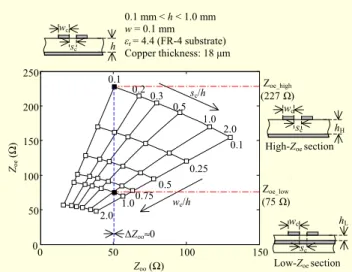
Figure 3 shows a Zoe-Zoo diagram of the microstrip coupled
lines used in the typical PCB applications. The width and
spacing of the lines are denoted by wc and sc, respectively. The
Fig. 3. Zoe-Zoo impedance diagram for design of high- and low-Zoe sections. wc sc h 0.1 mm < h < 1.0 mm w = 0.1 mm εr = 4.4 (FR-4 substrate) Copper thickness: 18 μm wc sc hH High-Zoe section wc sc hL Low-Zoe section 0 50 100 150 0 50 100 150 200 250 1.0 Zoe (Ω ) Zoo (Ω) wc/h sc/h 0.75 0.5 0.25 0.1 0.1 2.0 1.0 0.2 0.3 0.5 2.0 Zoe_high Zoe_low ΔZoo≈0 (227 Ω) (75 Ω)
Fig. 4. (a) Unit cell of VSI-EBG structure and (b) equivalent circuit model for deriving dispersion equations.
x y z ZoeL CM Port 1 CM Port 2 ZoeL ZoeL, βeL Half of TL for low-Zoe section
Via
Transmission line (TL) for high-Zoe section
Via
Half of TL for low-Zoe section
ZoeH, βeH ZoeL, βeL
Lvia Lvia
dL/2 dH dL/2
dL/2 dH dL/2
(a)
(b)
impedance diagram, the design parameters (wc, sc, hH, hL) can
be determined geometrically. Firstly, the Zoo value is
determined. A vertical line at the point where Zoo = 52 Ω,
denoted by the blue dotted line in Fig. 3, is drawn. Along this
line, the points of intersection can be used to determine the Zoe
values for the design of the VSI-EBG structure. To achieve the
wideband bandgap, the most distant Zoe values can be chosen.
The reason why the most distant values can increase the stopband bandwidth will be explained clearly in section III.
III. Dispersion Analysis
In this section, the dispersion equations of the proposed VSI-EBG structure are extracted to explain the principles of the CM
noise suppression by the bandgap and investigate the design parameter effects on the bandgap. For the dispersion analysis, the unit cell of the VSI-EBG structure is defined as shown in Fig. 4(a). The equivalent circuit model of the VSI-EBG unit cell for the even-mode propagation is developed as shown in Fig. 4(b).
For the even-mode propagation, the differential line and the corresponding patch can be modeled as the transmission line.
For instance, the high-Zoe section can be represented as the
transmission line having the length of dH, the even-mode
propagation constant of βeH, and the even-mode characteristic
impedance of ZoeH. The via structure is modeled as the via
inductance Lvia. To obtain the dispersion equations, the unit cell
is analyzed using the ABCD parameters, where the unit cell has
the length of dH+dL, the effective phase constant βeff, and the
characteristic impedance Zoeff. The ABCD parameters are given
by
high high
eff eff low low via
high high
eff eff low low
1 0 1 A B A B A B j L C D C D C D ω ⎛ ⎞ ⎛ ⎞ ⎛ ⎞⎛ ⎞ = ⎜ ⎟ ⎜ ⎟ ⎜ ⎟⎜ ⎟ ⎝ ⎠ ⎝ ⎠ ⎝ ⎠ ⎝ ⎠ low low via low low 1 0 1 A B j L C D ω ⎛ ⎞ ⎛ ⎞ ×⎜ ⎟⎜ ⎟ ⎝ ⎠⎝ ⎠, (1)
where the equation for the Lvia is used in [19] and ABCD
parameters are given by
(
)
(
)
(
)
(
)
eff eff eff eff
eff H L oeff eff H L
eff H L eff H L oeff cos ( ) sin ( ) , sin ( ) cos ( ) A B C D d d jZ d d j d d d d Z ⎛ ⎞ ⎜ ⎟ ⎝ ⎠ + + ⎛ ⎞ ⎜ ⎟ =⎜ + + ⎟ ⎜ ⎟ ⎝ ⎠ β β β β (2)
(
)
(
)
(
)
(
)
eL L oeL eL L low low low low eL L eL L oeL cos ( ) / 2 sin ( ) / 2 , sin ( ) / 2 cos ( ) / 2 d jZ d A B j C D d d Z β β β β ⎛ ⎞ ⎛ ⎞ ⎜= ⎟ ⎜ ⎟ ⎜ ⎟ ⎝ ⎠ ⎜ ⎟ ⎝ ⎠ (3)(
)
(
)
(
)
(
)
eH H oeH eH H high high high high eH H eH H oeH cos sin , sin cos d jZ d A B j C D d d Z β β β β ⎛ ⎞ ⎛ ⎞ ⎜ ⎟ = ⎜ ⎟ ⎜ ⎟ ⎝ ⎠ ⎜⎝ ⎟⎠ (4) H(L) o eff oeH(L) eff o eff H(L) 8 1 ln 2 4 h w Z w h ⎛ ⎞ = ⎜⎜ + ⎟⎟ π ⎝ ⎠ μ ε ε . (5)Evaluating the A component, we can obtain the dispersion equation for the analysis of the propagation characteristics and the design parameter effects on the bandgap.
oeH oeL eff H L eH H eL L oeL oeH oeH oeL eH H eL L oeL oeH via eH H eL oeH oeL 1 cos( ( )) 2 cos( ) 4 1 2 cos( ) 4 1 1 sin( 2 Z Z d d d d Z Z Z Z d d Z Z L d d Z Z β β β β β ω β β ⎛ ⎞ + = ⎜ + + ⎟ + ⎝ ⎠ ⎛ ⎞ + ⎜ − − ⎟ − ⎝ ⎠ ⎛ ⎞ − ⎜ + ⎟ + ⎝ ⎠
(
)
L via eH H eL L oeH oeL 2 via eH H eL L oeH oeL eH H eL ) 1 1 sin( ) 2 (cos( ) 4 cos( L d d Z Z L d d Z Z d d ω β β ω β β β β ⎛ ⎞ − ⎜ − ⎟ − ⎝ ⎠ + − − + L)). (6) Equation (6) can be approximated by ignoring the viainductance Lvia, which leads to removing the last three terms.
They have no significant effects on the bandgap in the
frequency of interest. In the paper, the Lvia is considered as only
the inductance of the shorting via structure for the sake of
simplicity. However, the Lvia is attributed to the entire physical
transition from a low-Zoe ground patch to a high-Zoe ground
patch. For a more exact Lvia value, a via inductance of a return
path and a mutual inductance between vias located at the same ground patch can be considered. The inductances are affected by the design parameters of the via diameter, the pitch between vias located at the same ground patch, the number of vias at the edge, and the setback distance from the center of the vias to the edge of the ground patch. To demonstrate the derived dispersion equation, the example structure is employed with
the parameters ZoeH/ZoeL = 2, Lvia = 0 nH, dH = 8 mm, and
dL= 8 mm. The parameter values are determined by
considering the implementation of the proposed VSI-EBG structure in the typical PCB applications. The propagation characteristic of the example VSI-EBG structure is calculated using the simplified dispersion of (6), as shown in Fig. 5. Clearly, it is found that the VSI-EBG structure forms the
bandgap between the lower cutoff frequency (fL) and the higher
cutoff frequency (fH). It is expected that the CM noise in the
bandgap of the VSI-EBG structure will be significantly suppressed, an effect experimentally verified in section IV.
The critical design parameters dH, dL, ZoeH, and ZoeL are
examined using the dispersion of (6). For the analysis of the
length ratio (dH/dL) effect, the example structure is considered
with the following values: dH+dL = 16 mm, ZoeH/ZoeL = 2, and
Lvia = 0.1 nH. The effects on the fL, fH, and stopband bandwidth
are investigated with variations of dH/dL from 0.1 to 10, as
shown in Fig. 6. The stopband bandwidth increases as the
dH/dL value approaches 1. Consequently, the stopband
bandwidth is maximized when the length of the high- and low-
Fig. 5. Dispersion diagram for VSI-EBG structure which illustrates stopband formed by periodic stepped impedance. 0 1 2 3 4 5 6 7 8 9 10 Frequency (GHz) Stopband βd (rad) Passband Passband fL fH 0 π/2 π -π /2 -π
Fig. 6. Effect of length ratio between high- and low-Zoeon cutoff frequencies and stopband bandwidth.
0 1 2 3 4 5 6 7 0 1 2 3 4 5 dH/dL St opband bandwidth (GHz) Proposed equation (6) Full-wave simulation (HFSS) Cutof f frequencies (GHz) 0.1 1.0 10 fH fL Bandwidth (Unit cell length) = 16 mm, ZoeH/ZoeL=2, Lvia=0.1 nH
Zoe sections are the same (that is, dH = dL). In addition to
maximizing the bandwidth, the other notable thing of the analysis results is that the considerable extension of the
stopband bandwidth is achieved by both a reduction in the fL
and an increase in the fH. A reduction in the fL implies that the
VSI-EBG structure that has a dH/dL value of 1 can have a
smaller unit cell size than VSI-EBG structures that have other
dH/dL values to achieve the same fL because the fL of a
periodic stepped impedance structure such as the VSI-EBG structure is inversely proportional to the unit cell length [18]. It is beneficial to the bandwidth enhancement and the size
reduction that the lengths of the high- and low-Zoe sections
become equal.
Fig. 7. Effect of impedance ratio between high- and low-Zoeon cutoff frequencies of bandgap.
1.0 1.5 2.0 2.5 3.0 0 1 2 3 4 5 6 7 8 9 10 ZoeH/ZoeL Cutof f frequencies (GHz) Proposed equations (7), (8) Full-wave simulation (HFSS) fH fL
(Unit cell length)=16 mm, dH=dL=8 mm, Lvia=0.1 nH
3.57 GHz 7.15 GHz
structure with dH = dL is considered due to the aforementioned
analysis result. Adding the assumption of the ignorable via
inductance and difference between βeL and βeH, (6) can be
extracted explicitly as the closed-form expression in the following.
p 1
L
H oeH oeL oeL oeH
1 8 cos 1 , 2 2 2 / / v f d Z Z Z Z − ⎛ ⎞ = ⋅ ⎜ − + + ⎟ ⎝ ⎠ π (7) p 1 H
H oeH oeL oeL oeH
1 8 2 cos 1 . 2 2 2 / / v f d Z Z Z Z − ⎛ ⎛ ⎞⎞ = ⋅ ⎜⎜ − ⎜ − ⎟⎟⎟ + + ⎝ ⎠ ⎝ π ⎠ π (8) Using (7) and (8), the impedance ratio effect is investigated
with the variations of the ZoeH/ZoeL value being from 1 to 3, as
shown in Fig. 7. The monotonic increase in the fH and the
reduction in the fL are shown as the ZoeH/ZoeL increases. From
the analysis result, it is found that the high ZoeH/ZoeL value needs
to be used to improve the stopband bandwidth. According to analysis results, it is predicted that the bandgap extend from 3.57 GHz to 7.15 GHz for the VSI-EBG structure with an impedance ratio value of 3. In section IV, the prediction is compared to the measurements using the VSI-EBG structure fabricated in the multilayer PCBs.
To validate (6) through (8), the results of the proposed equations are compared with the full-wave simulation results obtained using HFSS [20]. As shown in Figs. 6 and 7, the proposed equations are verified through agreement with the HFSS results.
From the analysis of the impedance ratio effect in Fig. 7, it is
found that the increasing difference between the hH and the hL
is beneficial to the stopband enhancement. However, the improvement is limited in practical PCB applications due to the inductance of the via structure. For the considerably high value
Fig. 8. Via inductance effect on cutoff frequencies of bandgap.
Lvia (nH) 0.001 0.01 0.1 1 10 fH fL 0 1 2 3 4 5 6 7 8 Cutof f frequencies (GHz) Bandwidth 0 1 2 3 4 5 6 7 8 9 10 St opband bandwidth (GHz) ZoeH/ZoeL=3
of the hH, the via inductance becomes a significant parameter
for the stopband bandwidth, and its effect cannot be ignored. In
Fig. 8, the via inductance effect on the fL and fH is added. Figure
8 depicts the limitation of the stopband bandwidth imposed by the large values of the via inductance. The variations of the cutoff frequencies with regard to the change of the via inductance is obtained using the dispersion of (6). As shown in
Fig. 8, the large value of the via inductance decreases in both fL
and fH. However, the decreasing rate of the fH is faster than that
of the fL, thus reducing the stopband bandwidth.
In summary, the effects of the main design parameters on the stopband enhancement are thoroughly investigated using the proposed dispersion equations throughout the section. As can be seen in Figs. 6 through 8, the performance of the VSI-EBG structure can be maximized by theoretical procedures and optimized for practical use in the high-speed PCBs.
IV. Experiment Results
To verify the proposed VSI-EBG structure in suppressing wideband CM noise, two test vehicles (TVs) are fabricated using the PCB process with the through hole via structure.
FR-4 (εr = 4.4, tanδ = 0.02) is used as a dielectric material. The
PCB process with the through hole via structure and the FR-4 material is well known as the manufacturing process for high-speed boards that bears a low cost and possesses high manufacturing reliability. TV A is designed as a reference structure. As shown in Fig. 9(a), TV A has differential lines on the solid ground without the VSI-EBG structure. TV B has the VSI-EBG structure for differential signaling, which consists of three copper layers, as shown in Fig. 9(b). The top layer is for
the differential line pair, the inner layer is for the low-Zoe
ground patches, and the bottom layer is for the high-Zoe ground
Table 1. Design parameters and dimensions for TV A and TV B.
Parameter Dimension (mm) Parameter Dimension (mm)
hH 0.9 sc 0.1
hL 0.1 t 0.018
dH 8.0 dvia 0.25
dL 8.0 wt 15
wc 0.1 - -
Fig. 9. TVs of (a) the differential line pair with solid ground plane (TV A) and (b) VSI-EBG structure (TV B).
Differential line pair (1st layer) Ground plane (2nd layer) hL t dL+dH width: wc, spacing: sc x y z x y z FR4 substrate (εr=4.4, tanδ=0.02) wt (a)
Differential line pair (1st layer) Low-Zoe patch (2nd layer) High-Zoe patch (3rd layer) hL hH t dL/2 dH dvia width: wc, spacing: sc x y z x y z FR4 substrate (εr=4.4, tanδ=0.02) wt (b)
B. The high-Zoe ground patch is connected with the low-Zoe
patch through two shorting via structures of which spacing is 1 mm.
The detailed design parameters and dimensions are as
follows: hH = 0.9 mm, hL = 0.1 mm, dH = 8 mm, dL = 8 mm,
wc = 0.1 mm, sc = 0.1 mm, t = 0.018 mm (t represents copper
thickness), dvia = 0.25 mm, and wt = 15 mm (wt represents total
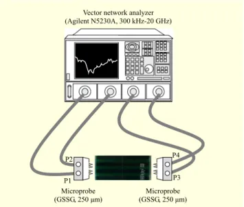
Fig. 10. Measurement setup using network analyzer and microprobes for differential lines with and without VSI-EBG structure.
Vector network analyzer (Agilent N5230A, 300 kHz-20 GHz) Microprobe (GSSG, 250 µm) (GSSG, 250 µm) Microprobe P1 P2 P3 P4
width). The values are determined to obtain the proper values
of the Zoe and Zoo using the design technique with the Zoe-Zoo
impedance diagram shown in Fig. 3. The low-Zoe and high-Zoe
values are 75 Ω and 227 Ω, respectively, while the Zoo value is
52 Ω with no changes along the differential lines, regardless of the vertically distributed ground patches. Using these impedance values and the dispersion equations derived herein,
the fL and fH can be predicted with 3.57 GHz and 7.15 GHz.
1. Measurements of CM Insertion Loss (Scc21)
The measured CM insertion loss (Scc21) of TV A and of TV B
is obtained using the four-port network analyzer with the GSSG 250 μm-pitch microprobes, as shown in Fig. 10. The use of the microprobes can minimize the parasitic effects of the additional structure for the measurement, such as the probe
pads (0.3 mm × 0.3 mm). The parasitic capacitance and
inductance of the probe pads are small enough to be ignored in the frequency range of the interest. The single-ended scattering parameters (S-parameters) at the four ports are measured. Then, the mixed-mode S-parameters are calculated using the
equations in [21] to obtain the Scc21.
As shown in Fig. 11, the proposed VSI-EBG structure significantly suppresses the CM noise in the frequency range from 3.4 GHz to 7.1 GHz (−10 dB suppression level). The wideband suppression is achieved with the suppression bandwidth of 3.7 GHz. It is experimentally proven that the VSI-EBG structure is valuable to mitigate the CM noise in differential lines even though a backward wave propagation at 4.5 GHz, which is caused by the inductance of the via structure
Fig. 11. Measurements of CM insertion loss for TV A (differential line pair without VSI-EBG structure) and TV B (VSI-EBG structure). 0 1 2 3 4 5 6 7 8 9 10 –45 –40 –35 –30 –25 –20 –15 –10 –5 0 Measured |S cc2 1 | (d B) Frequency (GHz) TV A (Reference) TV B (VSI-EBG) 3.4 GHz - 7.1 GHz 3.57 GHz - 7.15 GHz Dispersion equation Measurement
and the capacitance between the high- and low-Zoe ground
patches, degrades the suppression characteristics from the bandgap. The backward wave mode can be minimized by increasing in the via diameter, which leads to reduction in the via inductance. The result of the CM noise suppression was predicted in the dispersion analysis shown in the previous
section. As shown in Fig. 6, the fL and fH are estimated to be
3.57 GHz and 7.15 GHz, respectively. The estimated values from the proposed dispersion equation have desirable
correlations with the measured Scc21.
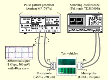
2. Measurements of CM Noise Suppression
To demonstrate the CM noise suppression, the CM noise is inserted through Ports 1 and 2 of the TVs and the amplitude of CM noise at Ports 3 and 4 is measured, as shown in Fig. 12. The CM noise inserted into TVs is generated by the differential pulse trains (101010 pattern, 2 Gbps, 500 mV) with the 40 ps intra-pair skew caused by the delay line. The CM noise used here mimics the wideband noise, which can be induced by the imbalance of the length in the practical differential channels and the cables. The measured amplitude of the CM noise is defined as half of the sum of the differential pulse trains at Ports 3 and 4, acquired using a sampling oscilloscope (Tektronix, TDS 8000B).
In Fig. 13, the experiment results demonstrate that the amplitude of the CM noise voltage is significantly reduced by the VSI-EBG structure (TV B), from 240 mV to 40 mV, notable compared to the differential line pair without the VSI-
Fig. 12. Measurement setup to demonstrate wideband suppression of CM noise caused by unbalanced differential channel.
Microprobe (GSSG, 250 µm) (GSSG, 250 µm) Microprobe P1 P2 P3 P4 Pulse pattern generator
(Anritsu MP1767A) Samplingoscilloscope (Tektronix TDS8000B) Test vehicles Differential signal (1 Gbps, 500 mV) with 40 ps skew
Fig. 13. Comparison of measured CM noise amplitudes in which CM noise is significantly reduced by VSI-EBG structure. 0 0.5 1.0 1.5 2.0 2.5 3.0 –200 –100 0 100 200 Time (ns) CM noise amplitude (mV) TV A (Reference) TV B (VSI-EBG) 240 mV (TV A) 40 mV (TV B) 1.0 ns
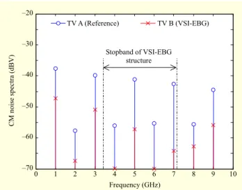
EBG structure (TV A). An 83% reduction in the peak-to-peak voltage of CM noise is achieved. Through the frequency spectrum, the significant mitigation of the CM noise can be clearly explained. In Fig. 14, the CM noise spectra for TV A and TV B are obtained using the fast Fourier transform (FFT) of the measured CM noise voltage. In the FFT result for TV A, a significant amount of the noise harmonics can be shown. The fundamental frequency of the CM noise is 1 GHz, associated with the CM noise period of 1 ns, shown in Fig. 13. For TV A, the spectra of the CM noise extend in the wideband frequency range. On the other hand, it is shown that the noise harmonics are suppressed over the wideband frequency range for TV B. Particularly, the noise harmonics from 4 GHz to 7 GHz are considerably mitigated by the bandgap of the VSI-EBG
Fig. 14. CM noise spectra for TV A and TV B which shows wideband suppression of CM noise of VSI-EBG structure. 0 1 2 3 4 5 6 7 8 9 10 –70 –60 –50 –40 –30 –20 TV A (Reference) TV B (VSI-EBG) Frequency (GHz) CM noise spectra (dBV) Stopband of VSI-EBG structure
structure. The relatively low suppression of the noise harmonics at 5 GHz is due to the anti-resonant peak, as mentioned in Fig. 11. However, the suppression characteristics of the CM noise voltage are not significantly affected by the resonant peak because the resonant peak can influence only a single harmonic and the suppression level is still more than 10 dB. It is experimentally verified that the wideband suppression of the CM noise using the VSI-EBG structure can be achieved in the multilayer PCBs, which ensures low cost, high manufacturing reliability, and high design flexibility. 3. Measurements of Differential Characteristics
In the previous section, the CM characteristics of the VSI-EBG structure are thoroughly examined through the experiment results. In this section, we will explore the differential characteristics of the VSI-EBG structure through
measurements of the differential-mode insertion loss (Sdd21) and
the eye diagram. Firstly, the measurement setup and the
experiment results for the Sdd21 will be discussed. The
measurement setup for Sdd21 is the same as the aforementioned
measurement setup for Scc21. From the measured S-parameters
at four single-ended ports, the Sdd21 can be calculated using the
mixed-mode S-parameters [21].
The measured Sdd21 of TV B (VSI-EBG structure) is
compared to the measurement of TV A (reference), as shown
in Fig. 15. TV B has no significant degradation of the Sdd21
except in the frequency range from 5 GHz to 6 GHz. In this
frequency region, the difference in the Sdd21 between TV A and
TV B is less than 0.7 dB on average. The amount of Sdd21
degradation is so small and its bandwidth is relatively narrow compared to the frequency spectra of high-speed differential
Fig. 15. Measurements of differential insertion loss for TV A and TV B. –10 –8 –6 –4 –2 0 Measured |S dd21 | (d B) 0 1 2 3 4 5 6 7 8 9 10 Frequency (GHz) TV A (Reference) TV B (VSI-EBG)
Fig. 16. Photograph of measurement setup to verify differential characteristics of VSI-EBG structure.
Differential probe (GSSG, 250 µm) Differential probe (GSSG, 250 µm) TV Pulse pattern generator (12.5 Gbps) Oscilloscope (20GS) Probe pads on test vehicle
data. Accordingly, no significant deterioration of the differential characteristics for TV B can be expected.
To demonstrate the differential signal integrity (SI) performance of TV B, another measurement for the eye diagram in the time domain is conducted. As shown in Fig. 16, the high-speed differential data launched from the pulse pattern generator is inserted into the TVs, and the eye diagram is measured using the sampling oscilloscope. The non-return to
zero data pattern with a 27−1 pseudorandom bit sequence is
used. The measurements are performed for the two cases of the data rates, namely 3.4 Gbps and 5.0 Gbps. The data rates are adopted, considering the application of the HDMI and USB 3.0. Note that the modulation and the coding technique for the HDMI and USB 3.0 are excluded in the measurement setup.
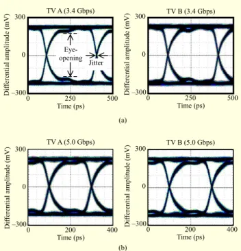
The experiment results of the eye diagram are compared in Fig. 17, and the eye opening voltage and the peak-to-peak jitter
Fig. 17. Measurements of eye diagram for differential data with (a) 3.4 Gbps and (b) 5.0 Gbps. Dif ferential amplitude (mV) 0 300 –300 Time (ps) 0 250 500 TV A (3.4 Gbps) Dif ferential amplitude (mV) 0 300 –300 TV B (3.4 Gbps) Time (ps) 0 250 500 Eye-opening Jitter (a) Dif ferential amplitude (mV) 0 300 –300 Time (ps) 0 200 400 TV A (5.0 Gbps) Dif ferential amplitude (mV) 0 300 –300 TV B (5.0 Gbps) Time (ps) 0 200 400 (b)
are summarized in Table 2. For both data rates of 3.4 Gbps and 5.0 Gbps, the eye diagrams of TV B perform better than the eye diagrams of TV A. As shown in Table 2, it is proven that the differential characteristics of TV B are not degraded compared to TV A in terms of the eye opening voltage and the peak-to-peak jitter.
Summarizing the results in this section, it is experimentally verified that the application of the VSI-EBG structure to the high-speed differential signals in the multilayer PCBs can achieve the wideband suppression of the CM noise induced by the imbalance of the differential channels. Further, it is not necessary to sacrifice the differential SI performance. Even though it requires the multilayer and the via structures, the VSI-EBG structure can be a valuable alternative to handle CM noise in high-speed PCBs, providing wideband CM noise suppression at a low cost and with high design flexibility.
V. Conclusion
We presented the application of the VSI-EBG structure to differential signaling for wideband CM noise suppression in the GHz frequency range. To analyze the proposed EBG structure for differential signaling, a dispersion equation was derived herein, which allowed for easy prediction of the bandgap and intuition of the design parameter effects. The performance of the proposed structure was experimentally verified for one differential line pair. However, the proposed structure can easily be extended to a few differential line pairs
Table 2. Summary of measured eye opening voltages and peak-to-peak jitters for TV A (reference) and TV B (VSI-EBG).
Data rate: 3.4 Gbps Data rate: 5.0 Gbps
TV A TV B TV A TV B
Eye opening
voltage (mV) 343 354 343 354
Peak-to-peak
jitter (ps) 14 14 15 16
for multichannel applications because the idea of the VSI-EBG structure is not dedicated to a single differential line pair. For further study, the crosstalk among differential line pairs as well as the noise suppression must be considered. The use of slotted patches or high dielectric constant material can be considered for the size reduction. The miniaturized VSI-EBG structure can apply to consumer electronics with a small form factor, such as mobile phones, tablet devices, and so on.
Acknowledgment
The authors would like to thank the anonymous reviewers for their constructive and valuable comments.
References
[1] F. Jun et al., “Signal Integrity Design for High-Speed Digital Circuits: Progress and Directions,” IEEE Trans. Electromagn.
Compat., vol. 52, no. 2, May 2010, pp. 392-400.
[2] G. Shiue et al., “Noise Reduction Using Compensation Capacitance for Bend Discontinuities of Differential Transmission Lines,” IEEE Trans. Adv. Packag., vol. 29, no. 3, Aug. 2006, pp. 560-569.
[3] J. Poltz, J. Beckett, and M. Josefsson, “Measurement and Simulation of Differential Skew in Twisted Pair Cables,” Proc.
55th Int. Wire Cable Symp., Providence, RI, USA, Nov. 12-15,
2006, pp. 141-146.
[4] C. Sreerama, “Effects of Skew on EMI for HDMI Connectors and Cables,” Proc. IEEE Int. Symp. Electromagn. Compat., vol. 2, Aug. 2006, pp. 452-455.
[5] B. Archambeault, J.C. Diepenbrock, and S. Connor, “EMI Emissions from Mismatches in High Speed Differential Signal Traces and Cables,” IEEE Int. Symp. Electromagn. Compat., July, 2007, pp. 1-6.
[6] T.-L. Wu et al., “A Novel Wideband Common-Mode Suppression Filter for Gigahertz Differential Signals Using Coupled Patterned Ground Structure,” IEEE Trans. Microw.
Theory Tech., vol. 57, no. 4, Apr. 2009, pp. 848-855.
Filter for GHz Differential Signals Using Periodic Defected Ground Plane,” IEEE Microw. Wireless Compon. Lett., vol. 18, no. 4, Apr. 2008, pp. 248-250.
[8] D. Sievenpiper et al., “High-Impedance Electromagnetic Surfaces with a Forbidden Frequency Band,” IEEE Trans. Microw. Theory
Tech., vol. 47, no. 11, Nov. 1999, pp. 2059-2074.
[9] R. Abhari and G.V. Eleftheriades, “Suppression of the Parallel-Plate Noise in High-Speed Circuits Using a Metallic Electromagnetic Band-Gap Structure,” IEEE MTT-S Int. Microw.
Symp. Dig., June 2002, pp. 493-496.
[10] J. Choi et al., “Noise Isolation in Mixed-Signal Systems Using Alternating Impedance Electromagnetic Bandgap (AI-EBG) Structure-Based Power Distribution Network (PDN),” IEEE
Trans. Adv. Packag., vol. 33, no. 1, Feb. 2010, pp. 2-12.
[11] J. Park et al., “Double-Stacked EBG Structure for Wideband Suppression of Simultaneous Switching Noise in LTCC-Based SiP Applications,” IEEE Microw. Wireless Compon. Lett., vol. 16, no. 9, Sept. 2006, pp. 481-483.
[12] M. Kim et al., “Vertical Inductive Bridge EBG (VIB-EBG) Structure With Size Reduction and Stopband Enhancement for Wideband SSN Suppression,” IEEE Microw. Wireless Compon.
Lett., vol. 22, no. 8, Aug. 2012, pp. 403-405.
[13] M. Kim et al., “A Compact and Wideband Electromagnetic Bandgap Structure Using a Defected Ground Structure for Power/Ground Noise Suppression in Multilayer Packages and PCBs,” IEEE Trans. Electromagn. Compat., vol. 54, no. 3, June 2012, pp. 689-695.
[14] F. de Paulis et al., “Design of a Common Mode Filter by Using Planar Electromagnetic Bandgap Structures,” IEEE Trans. Adv.
Packag., vol. 33, no. 4, Nov. 2010, pp. 994-1002.
[15] M.H. Nisanci et al., “Optimum Geometrical Parameters for the EBG-Based Common Mode Filter Design,” Proc. IEEE Int.
Symp. Electromagn. Compat., Aug. 2012, pp. 526-531.
[16] C.-H. Tsai and T.-L. Wu, “A Broadband and Miniaturized Common-Mode Filter for Gigahertz Differential Signals Based on Negative-Permittivity Metamaterials,” IEEE Trans. Microw.
Theory Tech., vol. 58, no. 1, Jan. 2010, pp. 195-202.
[17] M. Kim et al., “Vertical Stepped Impedance EBG (VSI-EBG) Structure for Wideband Suppression of Simultaneous Switching Noise in Multilayer PCBs,” IEEE Trans. Electromagn. Compat., vol. 55, no. 2, Apr. 2013, pp. 307-314.
[18] R. Ludwig, RF Circuit Design Theory and Applications, Englewood Cliffs, NJ: Prentice-Hall, 2000.
[19] C.-L. Wang et al., “A Systematic Design to Suppress Wideband Ground Bounce Noise in High-Speed Circuits by Electromagnetic-Bandgap-Enhanced Split Powers,” IEEE Trans.
Microw. Theory Tech., vol. 54, no. 12, Dec. 2006, pp. 4209-4217.
[20] ANSYS, Inc., High Frequency Structure Simulator (HFSS). http://www.ansys.com
[21] W. Fan et al., “Mixed-Mode S-Parameter Characterization of
Differential Structures,” Proc. IEEE 11th Conf. Electron Packag.
Technol. Conf., Dec. 10-12, 2003, pp. 533-537.
Myunghoi Kim received his BS, MS, and PhD in electrical engineering from the Korea Advanced Institute of Science and Technology (KAIST), Daejeon, Rep. of Korea, in 2003, 2005, and 2012, respectively. He is currently a senior member of the engineering staff at ETRI, Daejeon, Rep. of Korea. His responsibility includes electromagnetic compatibility and RF interference for the spacecraft and the satellite systems. From 2005 to 2008, he was a researcher for signal integrity and EMC analysis of the missile electronic systems in the Agency for Defense Development (ADD), Daejeon, Rep. of Korea. He was a visiting researcher at Silicon Image, Inc., Sunnyvale, CA, USA, in 2011. He has authored or co-authored more than 30 technical papers published in refereed journals or conference proceedings on the topics of modeling, design, and measurement of SI/PI analysis and electromagnetic bandgap (EBG) structure.
Sukjin Kim received his BS in electrical and electronics engineering from Korea University, Seoul, Rep. of Korea. He then advanced to Seoul National University, Seoul, Rep. of Korea, where he received his MS in electrical engineering. He is currently pursuing his PhD in electrical engineering from the Korea Advanced Institute of Science and Technology, Daejeon, Rep. of Korea. His current research interests include chip-package printed circuit board wireless power transfer co-design and co-simulation.
Bumhee Bae received his BS and MS in electrical engineering from the Korea Advanced Institute of Science and Technology (KAIST), Daejeon, Rep. of Korea, in 2009 and 2011, respectively. He is currently pursuing his PhD in electrical engineering from KAIST. His current research interest is the PI/SI/EMC of mixed-mode systems with chip-package PCB hierarchical structures.
Jonghyun Cho received his BS, MS, and PhD in electrical engineering from the Korea Advanced Institute of Science and Technology (KAIST), Daejeon, Rep. of Korea, in 2008, 2010, and 2013, respectively. He is currently working at KAIST as a postdoctoral researcher. His current research interest is electrical design in 2.5D and 3D IC. He is a specialist in noise coupling analysis and reduction in TSV-based 3D IC.
Joungho Kim received his BS and MS in electrical engineering from Seoul National University, Seoul, Rep. of Korea, in 1984 and 1986, respectively, and his PhD in electrical engineering from the University of Michigan, Ann Arbor, MI, USA, in 1993. In 1994, he joined the Memory Division of Samsung Electronics, where he was engaged in Gbit-scale DRAM design. In 1996, he moved to the Korea Advanced Institute of Science and Technology (KAIST). He is currently the Electrical Engineering Department chair at KAIST. Also, he is the director of the 3DIC Research Center (3DIC-RC), supported by Hynix Inc., and the Smart Automotive Electronics Research Center (SAE-RC), supported by KET Inc. He has authored or co-authored over 370 technical papers published in refereed journals or conference proceedings on the topics of modeling, design, and measurement of 3D IC, SiP, PCB, and wireless power transfer. Also, he has given more than 174 invited talks and tutorials at academic institutes and industry venues.
Jaehoon Kim received his PhD in computer engineering from Chungbuk National University, Cheongju, Rep. of Korea, in 2001. He joined ETRI in 1983, where he was involved in developing the Intelligent Network and KOREASAT projects. From 1992 to 1994, he was an OJT engineer at Martra-Marconi Space in the UK for the KOREASAT Project. From 1995 to 1999, he participated in the KOMPSAT-1 Ground Mission Control project as a principle member of the engineering staff in system engineering. From 2000 to 2012, he participated in the KOMPSAT-2, the COMS-1, the KOMPSAT-3, and the KOMPSAT-5 Ground Mission Control projects as the team leader. His research interests are security in satellite communications, fault diagnosis of satellites using AI technologies, and satellite navigation technologies.
Do Seob Ahn received his BS and MS in electronics engineering from Kyungpook National University in 1988 and 1990, respectively, and his PhD in radio science and engineering from Chungnam National University in 2010. He has worked for ETRI, Daejeon, Rep. of Korea, since 1990. He is currently the director of the Satellite Wireless Convergence Research Division of ETRI, working in the area of satellite wireless communication.