55-2 / J. Chang
IMID 2009 DIGEST •
Abstract
Resist patterning of all layers in TFT and BM layer in CF were carried out using UV-imprinting Lithography to make a 12.1 inch TFT-LCD panel at the resolution of 1280 x 800 lines (125 ppi). Technical challenges and solutions for resist patterning by UV-imprinting are shown in this article.
1. Introduction
Display industry has developed the various patterning technologies for the low cost and high volume production process. Moreover, the enormous investment cost caused by the increasing glass size accelerates the necessity of new patterning technology development. Inkjet printing, roll printing, and imprinting are the breakthrough candidates which can replace photolithography used in current TFT-LCD manufacturing. Display R&D Center (LCD Business., Samsung Electronics Co.) is working towards new patterning technology development and imprinting is one of them. Imprinting has been known to replicate the high resolution pattern with a high fidelity and a low cost equipment. Our research center had developed and exhibited the 2.46” QVGA transflective TFT-LCD panel which has an imprinted organic lens array layer for increasing reflectance[1]. On the basis of this one layer imprinting technology, our research has been extended to the resist patterning for all layers in TFT and BM layer in CF. The fabrication of 12.1” WXGA(1280×800) TN Mode TFT-LCD panel was achieved as a result of development of Imprinting resist patterning.
2. Result and Discussion
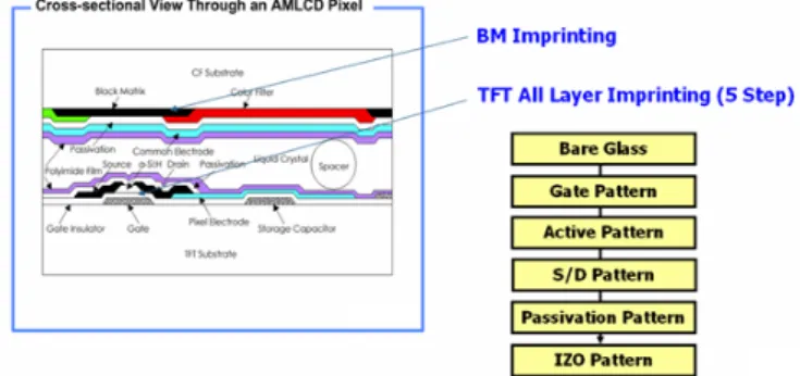
Conventional photolithography has been replaced with imprinting to pattern the resist material as shown in Figure 1. Resists for 5 layers from gate to pixel in TFT and 1 BM layer in CF were patterned by imprinting. The process for patterning each layer consists of 6 steps as follows; layer deposition, resist coating, Imprinting, ashing to remove residual layer, etching and resist strip. The process steps for patterning the layer using imprinting which replace photolithography are described in Figure 2.
Fig. 1. Cross sectional view through an AMLCD pixel. Imprinting was applied to resist patterning for 5 layers in TFT and 1 layer in CF.
During imprinting process development, the overlay accuracy, CD(Critical Dimension) uniformity, resolution and yield have been achieved and through these technical accomplishments, high quality TFT-LCD panel could be obtained.
All Layer Printed TFT-LCD Device by Large Area
UV-Imprinting Lithography
Jaehyuk Chang
1, Seung Jun Lee
1, Dae-Jin Park
1, Joo Han Bae
1, Sung Hee
Lee
1, Jangkyum Kim
1, Kyuyoung Kim
1, Jungmok Bae
2, Bo Sung Kim
1and Soonkwon Lim
11
LCD R & D Center, LCD Business., Samsung Electronics Co., LTD. San 24,
Nongseo-Dong, Giheung-Gu, Yongin-si, 449-711, KoreaTe.l: 82-31-209-9967 , E-mail: [email protected] 2
SAIT, Samsung Electronics Co., LTD., Yongin Si, Gyeonggi-Do, Korea
55-2 / J. Chang
• IMID 2009 DIGEST
Fig. 2. Schematic of process steps for patterning the layer using imprinting.
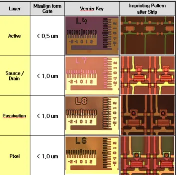
To allow the sufficient overlay accuracy, our effort has been focused on not only the improvement of tool’s performance but also development of process. As shown Figure 3, less than 1 um align accuracy with gate layer was obtained in the succeeding 4 layers.
Fig. 3. Align accuracy with gate layer and pattern scope image of the succeeding 4 layers (Active, S/D, Passivation, and Pixel).
Properties of imprinting resin and mold have been investigated with process factor. It was found that low viscosity of material was of great advantage to high throughput and residual uniformity. Material of 6 cP was used as imprinting resin. Microscopic level pattern pitch and high modulus of mold made it impossible to get conformal contact between mold
and substrate with variation of height due to the previous patterned layer(s) as seen in Figure 4. This non-conformal contact causes loss of some resist pattern during ashing process because the ashing should be applied till residual layer on the lowest part should be completely removed. To overcome this problem, compensation should be considered in master design.
Fig. 4. Pattern scope and SEM image after S/D imprinting. SEM image shows the different thickness residual layer in two points.
Particle contamination and bubble defect are the main factor relevant to the imprinting process yield. The influences of particle and bubble on pattern have been investigated respectively. It is found that particle generally contribute the source of the line short. Bubble, on the other hand, causes the line disconnection. Figure 5 is the picture of abnormal pattern caused by particle and bubble.
Through imprinting technology, it is expected that display industry realize high resolution pattern which enables to increase aperture ratio in TFT device. To introduce this advantage of imprinting to the industry, it is essential to fabricate the Master with fine pattern. Large size master(300mm x 400mm) with fine pattern which has 1 um space as channel length has been developed.
(a) (b)
Fig. 5. Abnormal patterns after imprinting process caused by (a) particle, and (b) bubble.
A A’ Point 1: 5000Å Point 2 A A’ Point 1: 5000Å Point 2
Layer Deposition Resist Coating Imprinting
Demolding Etch Strip
Layer Deposition Resist Coating Imprinting
55-2 / J. Chang
IMID 2009 DIGEST •
A sufficient quality of TFT was attained through Imprinting process and the prototype panel of 12.1” WXGA(1280×800) TN Mode TFT-LCD was achieved as shown Figure 6(a) and (b) respectively.
-20 -10 0 10 20 1E-15 1E-14 1E-13 1E-12 1E-11 1E-10 1E-9 1E-8 1E-7 1E-6 1E-5 Is d ( A m p ) Vgate (Volts) Imprinted TFT Photo TFT Ioff < 10-12A Ion > 10-6A -20 -10 0 10 20 1E-15 1E-14 1E-13 1E-12 1E-11 1E-10 1E-9 1E-8 1E-7 1E-6 1E-5 Is d ( A m p ) Vgate (Volts) Imprinted TFT Photo TFT Ioff < 10-12A Ion > 10-6A
Fig. 6. (a) Comparison of TFT properties from imprinting and photolithography, and (b) picture of the prototype panel of 12.1” WXGA(1280×800) TN Mode TFT-LCD[2].
Acknowledgements
Our research group has collaborated with Mechatronics & Manufacturing Technology Center in Samsung Electronics. We appreciate the technical support and comments from NND (Nano & Device) at the early stage of this research.
3. References
1. J. Bae, J. Chang, K. Kim, B. Kim, N. Noh, and S. Lim, Oral Presentation at International Conference
on Nanoimprint and Nanoprint technology
(NNT’08), Oct, 2008, Kyoto, Japan, “Large Area UV Nanoimprint Lithography for TFT-LCD Devices.”
2. Exhibited at 2008 FPD International, Oct, 2008, Yokohama, Japan.