61-3 / D.-Y. Shin
IMID 2009 DIGEST •
Abstract
Self-alignment for the fabrication of printed thin film transistors has become of great interest because of the resolution and registration limits of printing technologies. In this work, patterning and self-registration processes are introduced, which do not need surface energy patterning and the resulting minimum gate channel length could be down to 11.2 µm with the sheet resistance of 2.6 Ω/□ for the source and drain electrodes.
1. Introduction
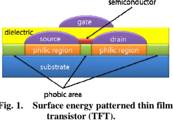
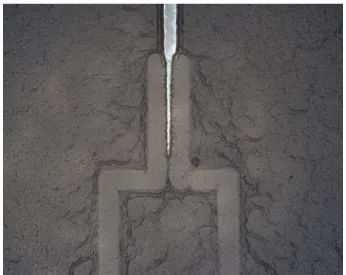
The fabrication of electronic and display components with printing technologies in lieu of conventional photolithographic processes has been of great interest by researchers and industries in the fields [1-3]. Because the current printing technologies have limited capabilities in terms of resolution and reliability, self-alignment has been explored [4-7]. However, self-alignment based on surface energy patterning requires multiple photolithographic processes to define surface energy differentiated regions, as shown in Fig. 1. In addition, surface energy patterning has no capability to prevent an electrical defect, i.e., short circuit, as shown in Fig. 2, where conducting ink in the source electrode region overflows and coalesces with the ink placed in the drain electrode region.
Fig. 1. Surface energy patterned thin film transistor (TFT).
When the deposition of the gate electrode is taken into consideration, it is required to be precisely placed between the source and drain electrodes but no surface energy differentiated regions exist after the deposition of a dielectric layer and hence additional photolithographic processes are required to define surface energy differentiated regions again.
In this work, novel patterning and self-registration processes are introduced, which not only eliminate the formation of short circuit but also provide the means to place the gate electrode precisely between the source and gate electrodes.
Fig. 2. Short circuit formation due to ink overflow over the gate channel region.
2. Experimental
Conducting polymer, the emeraldine form of polyaniline (Panipol X, Panipol Ltd., Finland), was spin-coated at 500 rpm for 20 sec on a glass microscope slide.
After drying and pattering it with a laser marker (U-5G, RMI Korea Co., Seoul, South Korea) to prepare regions of the source and drain electrodes, as shown in Fig. 3(a), organic silver was spin-coated on top of it at 500 rpm for 20 sec, as shown in Fig. 3(b).
After a hydrophobic layer was laid down at 3500 rpm for 20 sec, another laser exposure was made at the gate channel region between the source and drain electrode regions, as shown in Fig. 3(c).
Novel Method to Form Metal Electrodes by Self-Alignment
and Self-Registration Processes
Dong-Youn Shin
Nano-Mechanical Systems Research Division, Korea Institute of Machinery and Materials, Daejeon, 305-343, Republic of Korea
TEL:82-42-868-7378, e-mail: [email protected]
61-3 / D.-Y. Shin
• IMID 2009 DIGEST
Fig. 3. Schematic illustrations for the fabrication of self-patterned source/drain electrodes and self-registered gate electrode.
This laser exposure selectively and simultaneously removed polyaniline, organic silver and hydrophobic layers between the source and drain electrode regions and revealed the bare substrate.
After spin coating of silver/copper ink at 1500 rpm for 20 sec, the overall layers were cured at 170 ˚C for 5 min and then 210 ˚C for 10 min.
3. Results and discussion
It is found that the sheet resistance of the region where the cured organic silver layer stays alone is 2.57±0.06 Ω/□ but that of the region where polyaniline and organic silver layers are conjoined is
6.01±1.46 MΩ/□.
This finding that the conjunction of polyaniline and organic silver eventually becomes non-conductive is led by the chemical reaction and physical interaction between them. The initial sheet resistance of polyaniline in the emeraldine form is 362.8±22.2 Ω/□, as deposited. When organic silver is deposited on the polyaniline layer, however, the oxidation of polyaniline occurs and it becomes the non-conductive pernigraniline form [8,9]. The reduced silver seems to be embedded among non-conductive polyaniline granules and hence does not form a continuous conductive network.
This is the basic principle of self-patterning where conductive patterns are formed only where polyaniline is not present. If polyaniline is present, then no conductive patterns are formed even with conducting ink is present.
Another interesting point is the color change of polyaniline due to the change of the oxidation state. The light absorbance value of oxidized polyaniline increases about 6.3 times higher than those of polyaniline in the emeraldine form and organic silver at the wavelength of 532 nm. When hit by a laser, as shown in Fig. 3(c), polyaniline between the source and drain electrodes is selectively removed due to the enhanced light absorbance and hence the gate cavity could be formed. Fig. 4 shows the gate cavity formed with the above described procedures.
Fig. 4. Gate cavity formed between the source and drain electrodes.
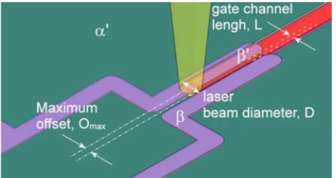
It is noteworthy that because of the optical transparency of organic silver and hydrophobic layers and the opaqueness of the polyaniline layer at the wavelength of 532 nm, the gate cavity is formed precisely in the middle of the source and drain
61-3 / D.-Y. Shin
IMID 2009 DIGEST •
electrode regions even when the laser beam position is deviated from the center of the source and drain electrode regions, as shown in Fig. 5. The tolerable maximum offset, Omax, becomes (D-L)/2, where D and
L are laser beam diameter and gate channel length,
respectively. This is the basic principle of self-registration, which removes the gate channel region only even with the laser beam position deviated.
Fig. 5. Maximum offset, Omax, of the gate electrode with laser assisted self-registeration.
Because the topmost hydrophobic layer in the gate channel region is selectively removed and the bare substrate is exposed, silver/copper nanoparticulate ink can be preferentially placed only at the gate channel region, as shown in Fig. 6. A printed top gate TFT could be made once suitable semiconducting and dielectric materials are placed in the gate cavity.
Fig. 6. Self-aligned source/drain electrodes and self-registered gate electrode.
4. Summary
The proposed self-patterning and self-registration processes have the novelties in the following aspects. Firstly, because of the oxidation state change of polyaniline, the conjoined region of polyaniline and organic silver becomes non-conductive. The region only where organic silver is placed without the presence of polyaniline becomes conductive and this
enables self-patterning free from short circuit formation. Secondly, the color change after the oxidation of polyaniline enhances the light absorbance value, which enables the selective removal of polyaniline at the gate channel region. Although the laser beam is not precisely positioned, the gate cavity could be formed precisely between the source and drain electrodes. This might alleviate the registration issue between the source/drain and the gate electrodes. By dropping semiconducting and dielectric inks into the formed gate cavity, a printed organic TFT could be made with the aid of patterning and self-registration.
5. References
1. D.A. Pardo, G.E. Jabbour and N. Peyghambarian,
Adv. Mater., 12, 1249 (2000).
2. K.E. Paul, W.S. Wong, S.E. Ready and R.A. Street,
Appl. Phys. Lett., 83, 2070 (2003).
3. Y. Liu, T. Cui and K. Varahramyan, Solid State
Electron., 47, 1543 (2003).
4. H. Sirringhaus, T. Kawase, R.H. Friend, T. Shimoda, M. Inbasekaran, W. Wu and E.P. Woo,
Science, 290, 2123 (2000).
5. H.-J. Kim, M. Almanza-Workman, A. Chaiken, W. Jackson, A. Jeans, O. Kwon, H. Luo, P. Mei, C. Perlov, C. Taussig, F. Jeffrey, S. Braymen and J. Hauschildt, IMID’06 Technical Digest, p.1539 (2006).
6. T. Arai, N. Sato, K. Yamaguchi, M. Kawasaki, M. Fujimori, T. Shiba, M. Ando and K. Torii, Jpn. J.
Appl. Phys., 46, 2077 (2007).
7. T. Fischer, U. Hahn, M. Dinter, M. Bartzsch, G. Schmidt, H. Kempa and A.C. Huebler, Org.
Electron., 10, 547 (2009).
8. J. Stejskal, J. Prokeš and I. Sapurina, Mater. Lett.,
63, 709 (2009).
9. J. Stejskal, M. Trchová, J. Kovářová, L. Brožová and J. Prokeš, React. Funct. Polym., 69, 86 (2009).