2441 Copyright ⓒ The Korean Institute of Electrical Engineers
This is an Open-Access article distributed under the terms of the Creative Commons Attribution Non-Commercial License (http://creativecommons.org/
An Injection-Locked Based Voltage Boost-up Rectifier for Wireless RF
Power Harvesting Applications
Ji-Hoon Lee*, Won-Jae Jung** and Jun-Seok Park
†Abstract
– This paper presents a radio frequency-to-direct current (RF-to-DC) converter for special RF power harvesting application at 915 MHz. The major featured components of the proposed RF-to-DC converter is the combination of a coupled rectifier and an active diode: first, the cross-coupled rectifier boosts the input voltage to desired level, and an active diode blocks the reverse current, respectively. A prototype was implemented using 0.18 μm CMOS technology, and the performance was proven from the fact that the targeted RF harvesting system’s full-operation with higher power efficiency; even if the system’s input power gets lower (e.g., from nominal 0 to min. -12 dBm), the proposed RF-to-DC converter constantly provides 1.47 V, which is exactly the voltage level to drive follow up system components like DC-to-DC converter and so on. And, maximum power conversion efficiency is 82 % calculated from the 0 dBm input power, 2.3 mA load current.Keywords:
Cross-coupled rectifier, LC tank, Active diode, Power harvesting system, RF-to-DC converter.1. Introduction
Driven by the trend of the Internet of Things (IoT) and the uninterrupted demand for Smart Wireless applications, Wireless Sensor Network (WSN) has become an important research area for both academic and industrial worlds. The bottleneck in wireless sensor network (WSN) implementation is the limited lifetime and frequent replacement of batteries used to supply the required electrical power for different nodes. Hence, energy harvesting is a key technique to solve this problem by remotely providing the required power to electronic circuitry [1].
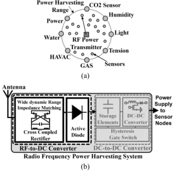
Recently, there have been various kinds of technical approaches to better self-sustained electrical/power devices/systems [2, 3]. In a field of WSN, regardless of its scale (house or building, etc.), the basic scheme of the entire system consists of [see Fig. 1 (a)]: a central stationary transceiver, a power transmitter, and multiple of sensor nodes. The central stationary transceiver is the top-level communication system. Under this transceiver’s control, the power transmitter energizes the dedicated sensor nodes containing the actual data such as humidity, light density, vibration, heat, and so forth.
So the power transmitter helps the sensor nodes to operate longer. It is our target to improve the power efficiency over distance between power transmitter and sensor nodes. In order to improve the power efficiency, one of the key components should be used: a RF-to-DC
converter and DC-to-DC converter. Now, within the sensor nodes, the level of harvested power from the power transmitter is in few micro watts (μW), and yet, the distance between the power transmitter and sensor nodes is desired to be longer. In such a case, the RF-to-DC converter requires two things: the higher RF-to-DC converter output, and power efficiency. Conventional RF-to-DC converter based on the CMOS full-bridge rectifier has a significant power loss [4]. Furthermore, its output voltage is limited by the peak of input voltage, while
† Corresponding Author: Dept. of Electrical Engineering, Kookmin University, Korea. ([email protected])
* Dept. of Electrical Engineering, Kookmin University, Korea. ({cz8700, jungwon}@kookmin.ac.kr)
Received: April 30, 2018; Accepted: August 19, 2018
(a)
(b)
Fig. 1. In a field of IoT: (a) RF power harvesting system;
(b) major blocks including proposed RF-to-DC converter
reverse current degrades the power efficiency. So the rectifier’s output voltage and power efficiency appears to be challenging.
The RF-to-DC converter scheme presented in this article first features a wide dynamic range impedance matching circuit and cross-coupled CMOS rectifier with LC tank; all set to realize the desired rectifier’s output voltage level. Then, the active diode is also featured in terms of blocking the reverse current. A prototype was implemented using 0.18 μm CMOS, and was integrated to test-aimed package fed by 35 dBm power transmitter at 915 MHz.
2. Proposed RF-to-DC Converter Design
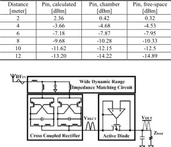
2.1 Some environmental conditions and case study By time, more sensor nodes were added to widen up the range of application, and so, the distance between power transmitter and the sensor nodes was issued: the longer the distance, the lower the input power the sensor node get. Therefore, the sensor node must be designed to operate even under low input power. In a view of above, a case study was conducted using well-known Friis formula [5], the calculated values of the input power versus distance was compared with the measured one [see Table 1].
First, we simulated the each block of the RF-to-DC converter [see Fig. 2] in air space. During this period, the calculated distance vs. input power values were used in designing the prototype. That is to say, we put the calculated values in simulation program, and use the entire simulation model to predict the overall operation. However, the measurement was still needed in order to build more precision model. The measurement was done in anechoic
chamber and free-space, where we put the simple scenario model comprised of: a high-precision signal generator and spectrum analyzer connected with respective omin-directional antenna (gain: 1dBi). The 35 dBm power was sent and received at 915 MHz, and the measured power was recorded per distance. As seen in Table 1, the difference between calculated and measured values of input power vs. distance is 2 dBm, which was taken into account as a power marginal value to design the wide dynamic range impedance matching circuit.
2.2 Components for rectifier output level: combined impedance matching circuit and cross-coupled rectifier
The proposed RF-to-DC converter consists of three stages [see again Fig. 2]: input impedance matching circuit with wide input power range, cross-coupled CMOS rectifier stage with LC tank and active diode stage.
When a specific maximum output power is desired, the impedance at the output must be matched to have a low impedance to achieve maximum output power. In other words, it seems to deliberately miss-match by matching the output matching element to any low impedance point rather than the inherent output impedance of the power element. Usually, the concept of matching is impedance matching that minimizes the reflection coefficient for each port such as S11 and S22. However, in a circuit requiring high output power, a low impedance that can output a maximum output power ‘Power Matching’ which is forced to match.
To do this, adjust the L and C values of the impedance matching unit to match the low impedance to ensure maximum output power
Consider comparing this feature with a conventional CMOS full-bridge rectifier consists of only two PMOS and two NMOS [6], it is dependent on the polarity of the input alternating current (AC) signal turn on or off the MOSFET combinations. The output voltage of this conventional CMOS full-bridge rectifier is attenuated by 2Vds, where Vds is the drain to source voltage of MOSFET. The Vds voltage drop and power loss due to the MOSFET’s turn on resistance degrade rectifier’s output power level and the power efficiency thereby [7]. For the ideal case each MOSFET device works as a zero loss switch and the rectified signal appears as the same strength of the input signal. As a result the output rectified signal appears as an attenuated version of the input signal. For a resistive load of RL, the rectification efficiency of a CMOS full bridge rectifier becomes, 2 m ds 2 m ds 2 m m 2V 2V V V 100% 8 100% V V 2 p p -æ ö ç ÷ æ - ö è ø ´ = ×ç ÷ ´ × æ ö è ø ç ÷ è ø (1)
Table 1. Comparison between calculated and measured
power from varying distance Distance [meter] Pin, calculated [dBm] Pin, chamber [dBm] Pin, free-space [dBm] 2 2.36 0.42 0.32 4 -3.66 -4.68 -4.53 6 -7.18 -7.87 -7.95 8 -9.68 -10.28 -10.33 10 -11.62 -12.15 -12.5 12 -13.20 -14.22 -14.89
where Vm and Vds are the peak values of the input
sinusoidal signal and the drain-to-source voltage drop of each conducting MOSFET, respectively. From Eq. (1) it is evident that lower the Vds value higher the rectifier
efficiency
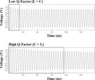
The referenced solution for this matter [8, 9] was a combination of the wide dynamic range impedance matching circuit and cross-coupled rectifier with LC tank, which not only rectifies its input AC signal but also boosts the converted DC output. Fig. 3 shows the schematic of wide dynamic range impedance matching circuit and cross-coupled rectifier. During the positive cycle of input AC signal, current flows towards the source terminal, charging the LC tank. Otherwise, LC tank supplies current to load. Therefore, the peak amplitude of output voltage of rectifier (VRECT) becomes higher than that of input AC signal [see Fig. 7(b)]. There is an initial settling time when the input voltage is boosted in the LC tank. This is related to the Q factor, which is simulated at about 3ns for the settling type and about 12ns for the high Q
In this system, the low Q is designed to bring the settling short, and the Q value is about 5 [see Fig. 4].
2.3 Component for blocking reverse current: active diode
Now, the next goal was block the reverse current while maintaining minimal voltage drop and power loss; and at this moment, the active diode was engaged. The active diode is comprised of a comparator and PMOS switch, as shown in Fig. 5 (a)[9]. The comparator detects the voltage difference between anode and cathode. In addition, it determines turn on or off state of the PMOS switch. When anode voltage is higher than cathode, the comparator output is low and PMOS switch is turned on. Otherwise, the PMOS switch is turned off and blocks the reverse current. Bulk of the PMOS switch is connected to cathode, so that the body diode helps pre-charging the load capacitor before PMOS switch turned on. Also the active diode and body diode block the reverse current from cathode to anode.
There are two power loss issues in active diode: the first one is the turn on resistance of PMOS switch. And another is the power consumption of the comparator. To reduce turn on resistance of PMOS switch, PMOS switch should be large. Note that the proposed active diodes hires PMOS switch with 10:1 μm width-to-length ratio. In order to reduce the power consumption of comparator, gm-enhanced technique is used [see Fig. 5 (b)], where R1 is connected to a DC tuning voltage (Vt). In the CMOS transistor gain factor is gmro. One conventional possibility
for gain improvement is utilization of cascade stage. However, this technique reduces the already small headroom available for signal swing in fine line technology.
Alternatively, improving the effective trans-conductance of a differential pair is one of the options to increase the transistor gain factor gmro. Proposed gm-enhanced
comparator adopt a tunable quasi floating gate (TQFG) as shown in Fig. 5 (b). This technique consist in connecting “weakly” the gates of transistors M2, M3 to the gates of
transistors M1, M4 through resistor R1 implemented with
minimum size diode connected transistor. M1 and M2 gate
voltage is equal and the effective trans-conductance gain at DC is gm,effDC=gm1+gm2. And gm,effAC=gm1/(1-gm2RL). This
allows us adjust the voltage of the gate-source terminal.
Fig. 3. Cross-coupled rectifier with LC tank scheme
Fig. 4. Simulation of LC tank settling time initially
(a) (b)
Fig. 5. Schematic of the (a) Active diode and (b)
Therefore, effective gm is improved, and eventually the power consumption is reduced.
3. Performance Evaluation
The prototype was implemented using 0.18 μm CMOS fabrication process, and this is shown in Fig. 6. The outline dimension is about 0.4 mm2. The RF-to-DC converter’s
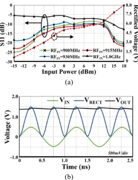
maximum output voltage is 8.02 V at matched frequency [see Fig. 7 (a)]. Fig. 7 (b) shows the input and output waveforms of the rectifier and RF-to-DC converter. The rectifier yields 1.5 V output when -12dBm input was given to the selected sensor node in the measurement. The RF-to-DC converter yields 1.47 V, which is sufficient enough to drive the follow up components within the sensor node [see again Fig. 1(b)]. The voltage drop is very small as 30 mV when compared to the rectifier output and RF-to-DC converter output.
Fig. 8 shows relationship between the output power and power efficiency per different load resistor (Rload) or input power (PIN). As load resistances increase, the output power decreases with increasing input power. With 0 dBm input power and 2 kΩ resistance, the measured output power is 580 uW. The efficiency of RF-to-DC converter is estimated or calculated by below Eq. (10):
2 out,RMS load out T in in in 0 V /R P η 1 P V (t) I (t) dt T = = ´ é ù ë û
ò
(2)where Vout,RMS is RMS value of output voltage, Rload is the
load resistance, Vin(t) and Iin(t) are the input voltage and current, respectively. And T is the period of on RF cycle. The maximum power efficiency is 77.8-82 % when the load resistor is 2 kΩ. The overall summary of prototype performance evaluation results are shown in Table 2.
A performance comparison of the RF-to-DC converter with prior art is presented in Table 3. The proposed architecture achieves a much wider optimal range and power efficiency compared to prior work.
More than ×1.4 improvement is achieved compared to the RF-to-DC converter [12]. Also, the proposed architecture
Fig. 6. Capture of implemented prototype
(a)
(b)
Fig. 7. Measurement results (a) S11 and rectified voltage
versus input power (b) RF-to-DC converter input and output waveform
Fig. 8. Prototype’s output power vs. power efficiency vs.
load resistances
Table 2. Measured prototype specifications
Parameter Value Unit
Input Frequency 915.00 MHz
Available Input Power Min. -12 dBm
VSWR 1.61 to 1.11 :1
RF-to-DC Converter Output 1.47 to 8.00 V
Power efficiency Max. 82.00 %
Voltage drop (VRECT to VOUT) 30.00 mV
Technology 0.18μm CMOS NA
Size 0.40 mm2
Table 3. Performance Comparison
ref Process Frequency Available Input power
Power efficiency This
work 0.18μm CMOS 915MHz -12dBm Max. 82% [7] 0.18μm CMOS 953MHz -12.5dBm Max. 67.5% [11] 0.18μm CMOS 900MHz -18dBm Max. 65% [12] 0.13μm CMOS 868MHz -21dBm Max. 60%
provides a wide optimal range without sacrificing neither the PCE as [7,11,12].
4. Conclusion
The proposed RF-to-DC converter’s minimal output voltage is 1.47 V, where input power is -12 dBm at 915 MHz. And, the maximal power efficiency is 82 % per 0 dBm power transmitter’s input power, where the load current is 2.3 mA. These results were found promising, and may contribute enhancing the power efficiency of the energy harvesting system. The better power efficiency the energy harvesting system has, the longer sensor nodes live. Finally, if the sensor nodes live longer, then the number of battery changes should be greatly reduced. Our future work may include: improve the power efficiency, when transmitter’s input power is set to lower than 0 dBm by any how (e.g., longer distance, low-power systems, etc.); drive the large load current while maintaining high power efficiency.
Acknowledgements
This work was supported by the Energy Technology program of the Korea Institute of Energy Technology Evaluation and Planning (KETEP) granted financial resource from the Ministry of Trade, Industry & Energy, Republic of Korea (No. 1415153755).
This work was supported by the Korea Institute of Energy Technology Evaluation and Planning(KETEP) granted financial resource from the Ministry of Trade, Industry & Energy, Republic of Korea in 2018(No. 20172410104800).
References
[1] Mansour Taghadosi; Lutfi Albasha; Nasir A. Quadir; Yousef Abo Rahama; Nasser Qaddoumi, “High Efficiency Energy Harvesters in 65nm CMOS Process for Autonomous IoT Sensor Applications,”
IEEE Access, vol. 6, pp. 2397-2409, Dec. 2017.
[2] Yoo, J., Long Yan, Seulki Lee, Yongsang Kim, and Hoi-Jun Yoo, “A 5.2mW Self-Configured Wearable Body Sensor Network Controller and a 12μW Wirelessly Powered Sensor for a Continuous Health Monitoring System,” IEEE J. Solid-State Circuits, vol. 45, no. 1, pp. 178-188, Jan. 2010.
[3] Junrui Liang, and Wei-Hsin Liao, “Improved Design and Analysis of Self-Powered Synchronized Switch Interface Circuit for Piezoelectric Energy Harvesting System,” IEEE Transctions, Industrial Electronics, vol. 59, no. 4, pp. 1950-1960, Apr. 2012.
[4] Peters C, Spreemsnn D, Ortmanns M , and Manoli Y.,
“A CMOS integrated voltage and power efficiency AC/DC converter for energy harvesting applica-tions,” J. Micromech. Microeng, vol. 18, no. 10, pp. 104005, Oct. 10.
[5] H. T. Friis., “A Note on a Simple Transmission Formula,” Proc. IRE, vol. 34, no 5, pp. 254-256, May 1946.
[6] Qingyun Ma, Haider, M.R., and Massoud, Y., “Low-loss rectifier for RF powering of implantable biosensing devices,” 13th IEEE Wireless and
Microwave Technology Conference, pp. 1-4, Apr.
2012.
[7] Kotani, K., Sasaki, A., and Ito, Takashi, “High-Efficiency Differential-Drive CMOS Rectifier for UHF RFIDs,” IEEE J. Solid-State Circuits, vol. 44, no. 11, pp. 3011-3018, Nov. 2009.
[8] Qingyun Ma; Mohammad Rafiqul Haider; Yehia Massoud, “A low-loss rectifier unit for inductive-powering of biomedical implants” 19th IEEE VLSI
and System-on-Chip (VLSI-SoC) International
Conference, pp. 86-89, Oct. 2011.
[9] Le, T.T., Jifeng Han, von Jouanne, A., and Mayaram, K., “Piezoelectric micro-power generation interface circuits,” IEEE J. Solid-State Circuits, vol. 41, no. 6, pp. 1411-1420, Jun. 2006.
[10] R. Yuan and D. P. Arnold, “An input-powered active AC/DC converter with zero standby power for energy harvesting applications,” in Energy Conversion
Congress and Exposition (ECCE), 2010 IEEE, pp.
4441-4446, Sept. 2010.
[11] S. Scorcioni, L. Larcher, A. Bertacchini, “A Reconfigurable Differential CMOS RF Energy Scavenger With 60% Peak Efficiency and -21dBm Sensitivity,” IEEE Microwave and Wireless
Com-ponents Letters, vol. 23, Issue 3, pp. 155-157, March
2013.
[12] L. B. A. Scorcioni and S. Larcher, “A reconfigurable differential CMOS RF energy scavenger with 60% peak efficiency and-21 dBm sensitivity,” IEEE Microw.
Wireless Compon. Letter, vol. 23, no. 3, pp. 155-157,
2013.
Ji-Hoon Lee He received a B.S. and
the M.S. in Electrical Engineering from Kookmin University, Seoul, Korea, in 2012, 2014. He has researched for Ph.D at Kookmin University, Seoul, Korea. He is interested in RF system, wireless communication systems, wire-less power transferring. Currently, his research is focused on designing CMOS rectifier and DC-to-DC converter for RF power harvesting applications for next generation wireless communication systems.
Won-Jae Jung He received a B.S.,
M.S. and Ph.D degrees in Electrical Engineering from Kookmin University, Seoul, Korea, in 2010, 2012, and 2018, respectively. Since March 2018, he has worked at Kookmin University Micro-wave Integrated Circuit Research Center, Seoul, Korea, where he is currently a Research Fellow. His current research interests RF power Systems.
Jun-Seok Park He received his B.S.
degree in Electrical Engineering from Kookmin University, Seoul in 1991 and his M.S. and Ph.D. degrees in
Electrical Engineering from the
Kookmin University in 1993 and 1996, respectively. In March 2003, he joined the Department of Electrical Engi-neering in Kookmin University, Seoul, Korea, where he is currently a professor. His principal area of research is smart grid, wireless power system, Electric Vehicle(EV) battery management systems.