P1-57 / K. H. Cho
IMID 2009 DIGEST •
Abstract
The fabrication of micro-scale irregular holes by using PMMA (Poly Methyl Methacrylate) beads in the front dielectric layer was proposed to improve luminous efficacy of an ac plasma display panel. Through the firing process of front dielectric layer, bowl shaped holes with a depth of 2.5µm, a top diameter of 8-12µm, and a bottom diameter of 4-7µm were fabricated. The proposed ac plasma display panel with the irregular micro-scale holes improved the luminous efficacy by 18 % due to the decrease in the minimum sustain voltage.
1. Introduction
Various studies to improve the luminous efficacy of ac PDPs have been conducted [1-3]; however, the application of these technologies to the commercial plasma display devices is not easy. An ac plasma display panel with a structure that included a micro capillary hole in the front dielectric layer was introduced and its characteristics were reported [3-4]. However, it was too large to apply the commercial plasma display devices with a front dielectric thickness of 30-40 µm, as the capillary hole has diameter of 75-125 µm, and depth of 30-75 µm [4-5].
Conventional ac plasma display panels use the coplanar dielectric barrier discharge (DBD) [6]. Plasma discharge and wall charge distribution on the dielectric surface is very important in the dielectric barrier discharge. Furthermore, the micro-scale distortion of the dielectric surface can have influence on the plasma discharge and wall charge distribution. Therefore, research on the fabricating micro-scale hole in the front dielectric layer for the distortion of the dielectric surface in the ac PDPs, and its discharge characteristics was needed.
2. Experimental
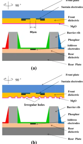
Fig. 1 shows the schematic diagram of ac PDPs
with (a) the conventional structure, and (b) the front dielectric of irregular holes. The coplanar gap between the common and scan electrodes is 80 µm and the width of the sustain electrode is 200 µm. The front and rear dielectric thicknesses are 40 µm and 20 µm, respectively, including a barrier rib height of 150 µm. The size of a sub-pixel is 1080×360 µm, and the gas mixture of Ne+13.5%Xe at 450 toor pressure was used as a discharge gas.
5.6 Front plate Sustain electrodes Front dielectric MgO Barrier rib Phosphor Address electrodes Rear dielectric Rear Plate 80µm (a) 90 ° Irregular holes Front plate Sustain electrodes Front dielectric MgO Barrier rib Phosphor Address electrodes Rear dielectric Rear Plate (b) 90 °
Fig. 1. Schematic diagram of ac PDPs with (a) the conventional structure, and (b) the front dielectric of irregular holes.
AC Plasma Display Panel with Irregular Micro-scale Holes in
the Front Dielectric Layer
Kwan Hyun Cho, Sung Il Ahn, Woo Hyun Kim and Kyung Cheol Choi
Dept. of Electrical Engineering, KAIST, Daejeon, KoreaTel.:82-42-350-8262, E-mail: [email protected]
P1-57 / K. H. Cho
• IMID 2009 DIGEST
3. Results and discussion
Fig. 2 shows SEM images of the irregular holes on the front dielectric layer of the top and cross-section. As shown in Fig. 2, micro-scale holes are positioned irregularly and the depth, top diameter, and bottom diameter are 2.5 µm, 8-12 µm, and 4-7 µm, respectively. Here, PMMA beads with a diameter of 5-7 µm were used, and also the MgO layer is properly deposited as shown in Fig. 2 (b).
(a) (b)
Fig. 2. SEM images of the irregular holes on the front dielectric layer. (a) Top view, (b) cross-sectional view of a hole.
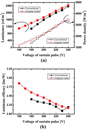
160 180 200 220 240 0 400 800 1200 1600 2000 2400 1000 2000 3000 4000 5000 P ow er dens ity [ W /m 2 ] L u m ina nce [cd /m 2 ]
Voltage of sustain pulse [V]
Conventional Irregular holes Conventional Irregular holes 160 180 200 220 240 2.00 2.25 2.50 2.75 3.00 3.25 L u mi nou s eff ica cy [lm /W ]
Voltage of sustain pulse [V]
Conventional Irregular holes
(a)
(b)
Fig. 3. (a) Luminance and power density, and (b) luminous efficacy in accordance with the voltage of sustain pulse.
The luminance, power density, and luminous efficacy in accordance with the voltage of sustain pulse are shown in Fig. 3. Here, the square voltage pulse with a frequency of 50 khz and the width of 4 µs was used. As shown in Fig. 3 (a), the power density and luminance are varied similarly; however, the minimum sustain voltage of 20 V in the dielectric structure with the irregular holes is decreased. As a result, the proposed ac plasma display panel with irregular micro-scale holes improved the luminous efficacy by about 18% due to the decrease in the minimum sustain voltage as shown in Fig. 3.
4. Summary
In this paper, irregular micro-scale holes were fabricated for application to commercial ac plasma display devices with a front dielectric thickness of 30-40 µm. An ac plasma display panel with irregular micro-scale holes in the front dielectric layer, improved the luminous efficacy due to a decrease in the minimum sustain voltage.
Acknowledgement
This work was supported by a Korea Science and Engineering Foundation (KOSEF) grant funded by the Korea government (MEST) (No. R11-2007-045-02001-0).
5. References
1. K. C. Choi, N. H. Shin, S. C. Song, J. H. Lee, S. D. Park, IEEE Trans. Electron Devices, Vol. 54, No. 2, pp210-218(2007).
2. G. Oversluizen, S. de Zwart, M. F. Gillies, T. Dekker, and T. J. Vink, Microelectron, J., vol. 35, no. 4, pp319-324(2004).
3. W. J. Chung, B. J. Shin, T. J. Kim, H. S. Bae, J. H. Seo, and K. W. Whang, IEEE Trans. Plasma Science, Vol. 31, no. 5, pp1038-1043(2006).
4. S. H. Park, K. S. Lee, B. J. Shin, S. Kim, K. H. Becker, and E. E. Kunhardt, SID Technical Digest, pp Displays, 5, pp1144-1177(2006).
5. D. I. Kim, S. Kim, W. Kokonaski, U.S. Patent No. 6, 545, 411 (Apr. 8 2003)
6. J.-P. Boeuf, J. Phys. D: Appl. Phys., vol.36, ppR53-R79(2003).