65-3 / B. H. Kim
IMID 2009 DIGEST •
Abstract
A novel a-Si TFT integrated gate driver circuit which suppresses the threshold voltage shift due to prolonged positive gate bias to pull-down TFTs, is reported. Negative gate-to-drain bias is applied alternately to the pull-down TFTs to recover the threshold voltage shift. Consequently, the stability of the circuit has been improved considerably.
1. Introduction
Monolithic integration of gate driver with a-Si TFTs on the glass substrate realizes simple module structure and cost reduction of AMLCDs. However the incessant threshold voltage (VT) shift of a-Si TFTs due
to prolonged positive gate bias is a critical problem of the a-Si TFT gate driver circuit. It is well known that both charge trapping into the gate insulator and trap state creation at the a-Si/SiN interface cause the instability [1], [2].
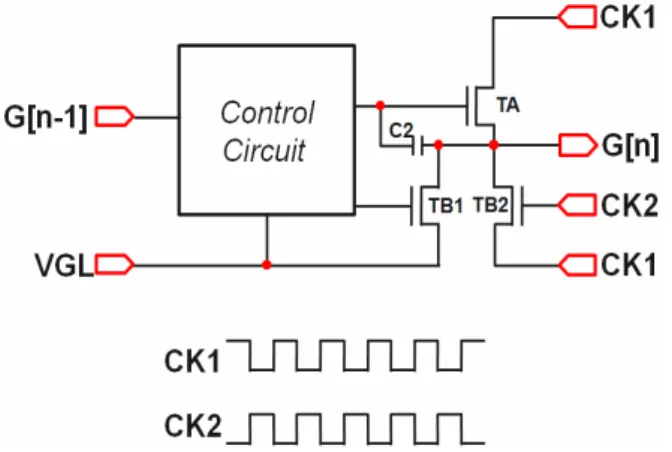
C. J. Shih et al. [3] invented a improved shift register circuit to solve this problem as shown in Fig. 1. They employed periodic negative gate-to-drain bias to one of the two pull-down TFTs, i.e. TB2. The negative gate bias recovers the positively shifted VT of
the pull-down TFT, TB2 by removing the trapped electrons in the gate insulator. Although it considerably enhances the stability of the gate driver, it is not enough because VT of the other pull-down
TFT, TB1 continues to shift. In this paper we propose a novel shift register circuit that applies negative gate-to-drain bias to both of the two pull-down TFTs to recover the VT shifts.
2. Novel gate driver
The novel gate driver that we developed is based on the dual pull-down a-Si gate driver designed by LG display to improve the stability of pull-down TFTs [4]. In this circuit, the two pull-down TFTs are turned on alternately so that the degradation of TFTs can be slowed down during long-term operation. Although the stability is rather enhanced, the VT shift problem
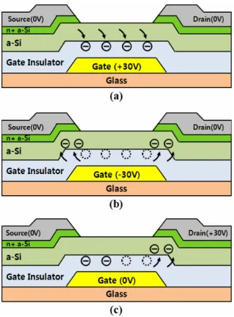
has not been completely resolved. The incessant charge trapping induced by the positive DC gate bias as shown in Fig. 2(a), is one of the factors which cause this problem.
However S. Y. Yoon et al. reported that the trapped electrons can be removed by negative gate bias as schematically shown in Fig. 2(b) leading to recovery of VT shift [5]. In addition we investigated the effect
of negative gate-to-drain bias with the gate and source short-circuited, i.e. positive drain bias with both the gate and source grounded as envisioned in Fig. 2(c). We found that the negative gate-to-drain bias restored the VT shift to some extent. Detailed experimental
results are presented in section 4.
Fig. 1. Schematic diagram of a prior shift register by C. J. Shih with negative gate-to-drain bias on one of two pull-down TFTs.
a-Si Gate Driver with Alternating Gate Bias to Pull-Down
TFTs
ByeongHoon Kim, JaeEun Pi, MinWoo Oh, Ren Tao, HwanSool Oh,
KeeChan Park
Dept. of Electronics Engineering, Konkuk University, HwaYang-Dong 1, GwangJin-Gu, Seoul 143-701, Korea
Tel.:82-2-450-4274, E-mail: [email protected]
65-3 / B. H. Kim
• IMID 2009 DIGEST
We propose a novel a-Si TFT gate driver circuit as shown in Fig. 3 that differs from the previous ones. Both of the two pull-down TFTs, M8A and M8B have negative gate-to-drain bias while they are turned off. The drain terminal – we consider the OUT[n] node as sources of M8A and M8B because the potential of OUT[n] is normally same or lower than the others – of each pull-down TFT is connected to alternating voltage sources VDD3 or VDD4 respectively, which is similar to the alternating supply voltages VDD1 and VDD2. Therefore relatively negative gate bias is applied to each pull-down TFT. We expect that the positive shift of VT is recovered by the negative gate
bias and that the stability of our new gate driver circuit is improved over long-term operation. Another two TFTs, M2A and M2B subject to periodic positive gate bias are also connected to VDD3 and VDD4 to suppress the VT shift.
3. Experimental
We investigated VT shift of a-Si TFTs due to
long-term positive gate bias and recovery effect by following negative gate-to-drain bias. a-Si TFTs with 100um wide and 5.5um long channel were used in the experiments.
Fig. 3. Schematic diagram of proposed shift register with alternating negative gate-to-drain bias on pull-down TFTs. Fig. 2. Charge trapping and detrapping in gate
insulator of a-Si TFTs (a) under positive gate bias, (b) negative gate bias and (c) negative gate-to-drain bias.
65-3 / B. H. Kim
IMID 2009 DIGEST • First, positive gate bias stress(VGS = 30V, VDS = 0V)
was applied to the TFTs for 100,000 seconds at 60 oC in air and in the dark. We measured the time evolution of TFT characteristics during the stress period e.g. at 10, 100, 1,000, 10,000, and 100,000 seconds.
After the stress, negative gate-to-drain bias (VGS =
0V, VDS = 30V) was applied to the TFTs for 100,000
seconds at 60℃ in air and in the dark. During this recovery process, we also measured the variation of the TFT characteristics.
4. Results and discussion
Figure 4 shows the experimental results of the stress and recovery processes. The transfer characteristics of the a-Si TFT moved to positive direction after the stress. This positive shift may be attributed to charge trapping in gate insulator and trap state creation in channel region. However the transfer characteristics moved back to negative direction after the recovery process. This indicates that the trapped charge in the gate insulator has been removed by negative gate-to-drain bias during the recovery process.
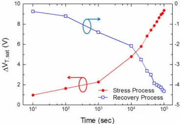
Figure 5 shows VT variation during the stress and
recovery process. VT of the TFT increased from
4.3V to 13.7V after the stress and decreased 4.4V after the following recovery process. The positive VT shift
is not fully recovered by the negative gate-to-drain bias because the trapped charges are not completely removed as illustrated in Fig. 2(c). The trapped charge
near the drain is detrapped by negative gate-to-drain bias(VGD = -30V) whereas the trapped charge near the
source remains without gate-to-source bias(VGS = 0V)
and because the trap states generated during stress period may remain.
Although the VT is not restored to the initial value,
one can see that our new gate driver suppresses VT
shift more effectively than the conventional dual pull-down a-Si gate driver having no recovery process.
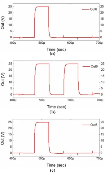
We investigated the effects of the three different characteristics, i.e. initial, stressed, and recovered TFTs on the circuit operation by SmartSpice simulations. The TFT characteristics were fitted employing the RPI a-Si TFT model(Level = 35) as envisioned in Fig. 6.
Figure 7(a) shows that the new gate driver operates normally with initial TFT model. However it exhibits malfunction with two output pulses (Fig. 7(b)) when the stressed TFT model is used for M2A, M2B, M8A, and M8B that are subject to periodic positive gate bias stress in the prior gate driver. It should be noted that the new gate driver restore normal operation as expected when the recovered TFT model is used for the four TFTs (Fig. 7(c)).
The simulation results in Fig. 7 indicate that the new gate driver having recovery process is more stable over prolonged operation than the prior gate driver with dual pull-down scheme only. The recovery process of negative gate-to-drain bias to the pull-down TFTs can be used in other a-Si gate drivers with similar structure.
Fig. 4. The transfer characteristics of a-Si TFT before and after 100,000 seconds positive gate bias stress(VGS =
30V, VDS = 0V) and after 100,000 seconds recovery
process(VGS = 0V, VDS = 30V).
Fig. 5. Time evolution of VT variation during 100,000 seconds gate bias stress and recovery process.
65-3 / B. H. Kim
• IMID 2009 DIGEST
5. Summary
We report a new dual pull-down a-Si TFT gate driver with enhanced stability by applying negative gate-to-drain bias alternately to the pull-down TFTs. According to our experimental results, the transfer characteristics of the a-Si TFTs exhibit positive shift after positive gate bias stress, however, they are restored to some extent by the recovery process, i.e. negative gate-to-drain bias. The simulation results show that our new gate driver has enhanced stability over long-term operation by suppressing the VT shift.
6. References
1. M. J. Powell, Apply. Phys. Lett., 43[6], p.597 (1983).
2. F. R. Libsch and J. Kanicki, Appl. Phys. Lett.,
62[11], p.1286 (1993).
3. C. J. Shih, C. Y. Hsu, C. C. Kuo, C. P. Ku, C.K. Yu, and C. H. Tsai, IDW’07, p.1897 (2007).
4. Binn Kim, Soo Young Yoon, LG Display, Korean Patent No. 10-2004-39136 (2004).
5. Soo Young Yoon, Yong Ho Jang, Binn Kim, Min Doo Chun, Hyung Nyuck Cho, Nam Wook Cho, Choong Yong Sohn, Sung Hak Jo, Chang-Dong Kim and In-Jae Chung, SID’05 Technical Digest, Vol. 36, p.348 (2005).
Fig. 6. Transfer characteristics of RPI a-Si TFT model fitted to measured characteristics and used in the SmartSpice simulation of the gate driver circuit.
Fig. 7. SmartSpice simulation results of the new gate driver with (a) initial, (b) stressed, and (c) recovered TFT model