Copyright © 2021 Techno-Press, Ltd.
http://www.techno-press.org/?journal=journal=anr&subpage=5 ISSN: 2287-237X (Print), 2287-2388 (Online) 1. Introduction
International Roadmap of Devices and Systems (IRDS) is a 15 years roadmap on the development and growth of electronic devices and systems in the micron and nanometer regime. The ‘more than Moore Chapter’ in IRDS, predicts that there is no more headroom for 2D geometry scaling and 3D very large-scale integration (VLSI) of circuits and systems using stacked integration approach after the year 2027 (IEEE 2018). Thus, this major challenge has urged the semiconductor industry to discover potential “more than Moore’ materials, in order to achieve higher computing power. Due to the success on the exploration of graphene (Novoselov et al. 2004), researchers are interested in studying and exploring other 2D materials, including silicene. Silicene is known as a potential 2D material besides graphene. It is a monolayer allotrope of silicon (Si) arranged in honeycomb lattice structure like graphene (Ding and Ni 2009). Moreover, the atomically thin 2D materials are postulated to enable a new generation of nanoelectronic devices, such as wearable and flexible electronics (Gupta et al. 2015, Chhowalla et al. 2016)
Silicene has similar Dirac cone properties and lattice structure like graphene, and these unique properties result in an ultra-high carrier mobility. Moreover, silicene has zero bandgap when the spin orbiting effect is neglected (Lew
Corresponding author, Ph.D., E-mail: [email protected]
Yan Voon et al. 2016). This unique characteristic can be observed in the electronic dispersion relation as shown in the published results from other researchers (Guzmán-Verri and Lew Yan Voon 2007, Ding and Wang 2013, Huang et al. 2013). Meanwhile, the mean free path (MFP) of monolayer silicene for acoustic and optical phonon scattering are 178 𝑛𝑚 and 29 𝑛𝑚 (Wang et al. 2015), respectively. The next generation devices might be able to operate under ballistic or near-ballistic transport due to these short MFP values (Arora et al. 2007). Furthermore, the valence band and conduction band of the pristine silicene touch each other at the 𝐾-point within the first Brillouin zone (Guzmán-Verri and Lew Yan Voon 2007, Ding and Wang 2013, Huang et al. 2013, Gert et al. 2015). This semimetallic property of silicene hinders its potential as a field-effect transistors (FETs) where the channel materials require band gap values between 0.4 𝑒𝑉 (Ni et al. 2014) and 3 𝑒𝑉 (Tang and Zhou 2013). Although graphene is an established 2D material with mature knowledge in the research community, silicene offers potential advantages in terms of the fabrication processes because Si-based technology is well known and dominant in the semiconductor industry (Tao et al. 2015).
Meanwhile, experimentalists are constantly working to explore practical fabrication procedures to produce silicene in the laboratory. Unlike graphene which can be mechanically exfoliated from its bulk graphite, molecular beam epitaxial (MBE) growth is identified as the most viable technique to fabricate silicene (Molle et al. 2018). In the past decade, most of the experimental work have been focusing on depositing silicene on metal substrates such as silver (Vogt et al. 2012)
Low-dimensional modelling of n-type doped silicene
and its carrier transport properties for nanoelectronic applications
M.W. Chuan, J.Y. Lau, K.L. Wong, A. Hamzah, N.E. Alias, C.S. Lim and M.L.P Tan
School of Electrical Engineering, Faculty of Engineering, Universiti Teknologi Malaysia, 81310 Skudai, Johor, Malaysia
(Received September 4, 2020, Revised January 4, 2021, Accepted January 5, 2021)
Abstract. Silicene, a 2D allotrope of silicon, is predicted to be a potential material for future transistor that might be compatible with present silicon fabrication technology. Similar to graphene, silicene exhibits the honeycomb lattice structure. Consequently, silicene is a semimetallic material, preventing its application as a field-effect transistor. Therefore, this work proposes the uniform doping bandgap engineering technique to obtain the n-type silicene nanosheet. By applying nearest neighbour tight-binding approach and parabolic band assumption, the analytical modelling equations for band structure, density of states, electrons and holes concentrations, intrinsic electrons velocity, and ideal ballistic current transport characteristics are computed. All simulations are done by using MATLAB. The results show that a bandgap of 0.66 𝑒𝑉 has been induced in uniformly doped silicene with phosphorus (PSi3NW) in the zigzag direction.
Moreover, the relationships between intrinsic velocity to different temperatures and carrier concentration are further studied in this paper. The results show that the ballistic carrier velocity of PSi3NW is independent on temperature within
the degenerate regime. In addition, an ideal room temperature subthreshold swing of 60 𝑚𝑉/𝑑𝑒𝑐 is extracted from ballistic current-voltage transfer characteristics. In conclusion, the PSi3NW is a potential nanomaterial for future
electronics applications, particularly in the digital switching applications.
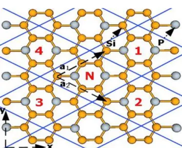
Fig. 1 Schematic lattice structure of 2D PSi3, a1 and a2
denotes the displacement vectors, each parallelogram shows a primitive unit cell of PSi3.
and gold (Stpniak‐Dybala et al. 2019). At any rate, the search for suitable non-metallic substrate is more favourable by the research community due to wider practical applications (Le Lay et al. 2018).
Recently, various bandgap opening techniques are studied in order to tune the semimetallic properties of silicene (Chuan et al. 2020b). For example, band gap opening techniques for 2D materials like substitutional doping (Lopez-Bezanilla 2014, Ma et al. 2014), incorporating defects (Gao, Zhang et al. 2013, Ali, Pi et al. 2017, Wong et al. 2019), strain engineering (Mohan et al. 2014, Voon et al. 2015) and others have been studied. Among all these techniques, substitutional doping is a typical way used in the semiconductor fabrication industry to design a device based on the desired applications (Taur et al. 1995).
This work is primarily motivated by the published DFT results (Ding and Wang 2013) where sizable band gap values are discovered in silicene by applying substitutional doping with n-type material, phosphorus (P) at a constant concentration, referred as PSi3 nanostructure in the article.
However, there is still lack of details on other important electronics properties and carrier transport properties for PSi3
nanostructure. In addition, theoretical and computational studies are relatively important (Bouadi et al. 2018) because there are still major challenges in the fabrications of free-standing silicene (Balendhran et al. 2015).
In this paper, an analytical model based on the tight-binding and parabolic band assumption is employed to investigate the essential electronic and carrier transport parameters of 1D PSi3 nanoribbon (PSi3NW) as shown in Fig.
1. In Section 2, the mathematical modelling of band structure, density of states (DOS), carrier concentration, intrinsic velocity and ballistic current-voltage (I-V) characteristics of PSi3NW
using nearest neighbour tight-binding (NNTB) approach and parabolic band assumption are shown. In Section 3, all the simulation results obtained are shown and analysed. Lastly in Section 4, the conclusion is drawn based on the findings of this work.
2. Mathematical modelling
2.1 Band structure and density of states of PSi3NW
Fig. 1 shows the sketched lattice diagram of the 2D PSi3
with the corresponding displacement vectors to its nearest neighbours, defined as 𝑎⃗⃗⃗⃗ and 𝑎1 ⃗⃗⃗⃗ . The PSi2 3 nanosheet is
assumed to be a perfect planar lattice structure. This assumption is employed because planar silicene has been successfully fabricated recently (Stpniak‐Dybala et al. 2019), despite the mainstream buckled structure. Every primitive unit cell interacts with its four nearest neighbour unit cells. The remaining displacement vectors in the opposite direction are the complex conjugate of 𝑎⃗⃗⃗⃗ and 1
𝑎2
⃗⃗⃗⃗ . For NNTB, the time-independent Schrödinger equation was applied in the matrix form (Datta 2005), given as
𝐸(∅0) = [ℎ(𝑘⃗ )](∅0) (1)
where 𝐸 is the energy, ∅0 and [ℎ(𝑘⃗ )] show the wave
function and the Hamiltonian operator in matrix form, respectively. The Hamiltonian operator matrix is obtained from the summation all non-zero overlap components for m in positive integers among all the nearest neighbour unit cells by using:
[ℎ(𝑘⃗ )] = ∑ 𝐻𝑛𝑚𝑒𝑖𝑘⃗ ∙(𝑟 𝑛−𝑟 𝑚) 4
𝑚=𝑛,1
(2)
where 𝑘⃗ as the wave vector, 𝐻𝑛𝑚 is the Hamiltonian
matrix for every neighbouring unit cell, 𝑟 𝑛 and 𝑟 𝑚 are the
position vectors used to determine the displacement of 𝑚𝑡ℎ
unit cell from 𝑛𝑡ℎ unit cell. The origin could be placed at
any atom of 𝑛𝑡ℎ unit cell. In this work, the 𝑛𝑡ℎ unit cell is
defined as the unit cell labelled letter ‘N’ in Fig 1. After obtaining the Hamiltonian matrices for unit cell: 𝐻𝑛𝑛 and
the nearest neighbours: 𝐻𝑛1, 𝐻𝑛2, 𝐻𝑛3, and 𝐻𝑛4, apply Eq.
(2) to obtain the complete Hamiltonian matrix as
[ℎ(𝑘⃗ )] = [ 𝐸𝑜𝑆𝑖 0 0 𝒕𝑷−𝑺𝒊 0 ℎ1∗ ℎ 2∗ 0 0 𝐸𝑜𝑆𝑖 0 𝒕𝑷−𝑺𝒊 0 0 𝑡𝑆𝑖−𝑆𝑖 ℎ1∗ 0 0 𝐸𝑜𝑆𝑖 𝒕𝑷−𝑺𝒊 0 𝑡𝑆𝑖−𝑆𝑖 0 ℎ2∗ 𝒕𝑷−𝑺𝒊 𝒕𝑷−𝑺𝒊 𝒕𝑷−𝑺𝒊 𝑬𝒐𝑷 0 0 0 0 0 0 0 0 𝑬𝒐𝑷 𝒕𝑷−𝑺𝒊 𝒕𝑷−𝑺𝒊 𝒕𝑷−𝑺𝒊 ℎ1 0 𝑡𝑆𝑖−𝑆𝑖 0 𝒕𝑷−𝑺𝒊 𝐸𝑜𝑆𝑖 0 0 ℎ2 𝑡𝑆𝑖−𝑆𝑖 0 0 𝒕𝑷−𝑺𝒊 0 𝐸𝑜𝑆𝑖 0 0 ℎ1 ℎ2 0 𝒕𝑷−𝑺𝒊 0 0 𝐸𝑜𝑆𝑖] (3) where ℎ1= 𝑡𝑆𝑖−𝑆𝑖𝑒𝑖(𝑎𝑘𝑥−𝑏𝑘𝑦) and ℎ2= 𝑡𝑆𝑖−𝑆𝑖𝑒𝑖(𝑎𝑘𝑥+𝑏𝑘𝑦).
𝐸𝑜𝑆𝑖 and 𝐸𝑜𝑃 represent the on-site or bounded energy for
Si and P atom, respectively, 𝑡𝑃−𝑆𝑖 is the hopping energy for
P-Si atoms, and 𝑡𝑆𝑖−𝑆𝑖 is the hopping energy for Si-Si
atoms. ℎ1∗ and ℎ2∗ is the complex conjugate of ℎ1 and
ℎ2, respectively. The bold terms in Eq. (3) show the
influence of doping atoms (P) to the Hamiltonian matrix of silicene.
Table 1 tabulates the NNTB parameters used in this work: 𝑡𝑃−𝑆𝑖 by fitting DFT result, 𝑡𝑆𝑖−𝑆𝑖 from (Chuan et
al. 2020a, Chuan et al. 2020c), and both the 𝐸𝑜𝑆𝑖 and 𝐸𝑜𝑃
from (Harrison 2004). After that, the band structure is assumed be confined in the x-direction as explained by (Lim, Hamzah et al. 2017b) to obtain 1D PSi3NW in the
zigzag direction. Then, Eq. (3) is substituted into Eq. (1) to obtain the energy eigenvalue equation. By solving the
Table 1 The compute NNTB model parameters for uniformly doped silicene
Parameters 𝑡𝑆𝑖−𝑆𝑖 𝑡𝑃−𝑆𝑖 𝐸𝑜𝑆𝑖 𝐸𝑜𝑃
Value (𝑒𝑉) -1.02 -1.16 -7.59 -9.54
energy eigenvalue equation using the equation: det |[ℎ(𝑘⃗ )] − 𝐸𝐼| = 0, the energy eigenvalues are obtained.
Next, to obtain a simple analytical model for carrier characteristics of PSi3NW (Lundstrom and Antoniadis
2014), parabolic band assumption is applied around the conduction band minimum (CBM) and valence band maximum (VBM) (Ismail et al. 2016) as these bands are the responsible for carrier flow in semiconductor. The parabolic band assumption originates from the effective mass equations such that the wave functions in the Schrödinger equation do not appear explicitly (Datta 1997) to simplify the modelling procedures, the parabolic band equations are
𝐸𝑒(𝑘) = 𝐸𝑐+ ħ2𝑘2 2𝑚𝑒∗ (4a) 𝐸ℎ(𝑘) = 𝐸𝑣− ħ2𝑘2 2𝑚ℎ∗ (4b) where 𝐸𝑐 and 𝐸𝑣 represent the energies at CBM and
VBM, respectively, 𝑚𝑒∗ and 𝑚ℎ∗ are the effective mass
for electrons and holes, respectively, and ħ = ℎ/(2𝜋) is the reduced Planck’s constant.
Density of states (DOS), describing the number of available states with respect to energy 𝐸, can be derived applying Eq. (5) to the parabolic band structure Eqs. (4a) and (4b) (Lim et al. 2017a), expressed as
𝐷𝑂𝑆(𝐸) = ∆𝑁𝑥 𝐿𝑥∆𝐸
(5) where Nx is the total number of states, Lx is the length and E is
the energy. The resulting DOS for carriers are obtained as
𝐷𝑂𝑆𝑒(𝐸) = √ 2𝑚𝑒∗ 𝜋2ħ2(𝐸 − 𝐸𝑐)−1 2⁄ (6a) 𝐷𝑂𝑆ℎ(𝐸) = √ 2𝑚ℎ∗ 𝜋2ħ2(𝐸𝑣− 𝐸)−1 2⁄ (6b)
where the DOS for electron (𝐷𝑂𝑆𝑒) and DOS for hole
(𝐷𝑂𝑆ℎ) are derived using Eqs. (4a) and (4b), respectively.
2.2 Carrier concentration of PSi3NW
In this subsection, the concentrations for electrons and holes in CBM and VBM are derived. The probability of the occupied states at a given temperature, T can be described by Fermi-Dirac distribution (Lundstrom and Jeong 2013)
𝑓(𝐸) = [1 + exp (𝐸 − 𝐸𝐹 𝑘𝐵𝑇
)]
−1
(7)
where 𝑘𝐵 represents the Boltzmann constant. Thermal
equilibrium or intrinsic electrons concentration (Jooq et al. 2018) available in the conduction band is calculated using
𝑛 = ∫ 𝐷𝑂𝑆𝑒(𝐸)𝑓(𝐸) 𝑑𝐸 ∞ 0 = 𝑁𝑐ℑ−1 2 ⁄(𝜂𝑐) (8) where ℑ−1 2
⁄ (𝜂𝑐) is the Fermi-Dirac integral (FDI) of order
−1/2 with respect to 𝜂𝑐, 𝑁𝑐 represents the effective DOS
of electrons in terms of normalised thermal energy, 𝜂𝑐 =
(𝐸𝐹− 𝐸𝑐)/𝑘𝐵𝑇, and is given by 𝑁𝑐= √(2𝑚𝑒∗𝑘𝐵𝑇)/𝜋ħ2.
The general equation for FDI of order 𝑗 (Kim and Lundstrom 2008) is given by ℑ𝑗(𝜂) ≡ 1 Γ(j + 1)∫ 𝜀𝑗 𝑑𝜀 1 + 𝑒𝜀−𝜂 ∞ 0 (9) where Γ denotes the gamma function. Eq. (9) is crucial and used throughout the rest of this paper. In a similar way, the intrinsic (which is also known as thermal equilibrium) holes concentration in the valence band can be calculated using
𝑝 = ∫ 𝐷𝑂𝑆ℎ(𝐸)[1 − 𝑓(𝐸)] 𝑑𝐸 0 −∞ = 𝑁𝑣ℑ−1 2 ⁄(𝜂𝑣) (10) where the effective density of states of holes, 𝑁𝑣, and
normalised energy in terms of thermal energy 𝜂𝑣 are given
by 𝑁𝑣 = √(2𝑚ℎ∗𝑘𝐵𝑇)/𝜋ħ2 and 𝜂𝑣= (𝐸𝑣− 𝐸𝐹)/𝑘𝐵𝑇 ,
respectively. Note that for holes concentration in the valence band, 𝑓(𝐸) is substituted by [1 − 𝑓(𝐸)] to compute the probability of empty states.
FDI usually can be separated and divided into two regimes which are non-degenerate and degenerate regimes that reduces Eq. (9) into ℑ𝑗(𝜂) = 𝑒𝜂 for (𝜂 < −2 )
regardless of 𝑗 and ℑ𝑗(𝜂) = 𝜂𝑗+1/[(j + 1)Γ(j + 1)] for
(𝜂 ≥ 3) respectively (Johari, Ahmadi et al. 2010). The numerical solutions for FDI in this work are based on the available Matlab function on nanohub.org (Kim and Lundstrom 2008).
2.3 Intrinsic carrier velocity of PSi3NW
From this subsection onwards, the focus is on the electrons as the carriers in the PSi3NW nanostructure. The
intrinsic velocity of electrons is obtained by dividing the total electrons velocity by the electrons concentration (Arora 2015), given as ∫ |𝑣𝑒(𝐸)|𝐷𝑂𝑆𝑒(𝐸)𝑓(𝐸) 𝑑𝐸 ∞ 0 ∫ 𝐷𝑂𝑆𝑒(𝐸)𝑓(𝐸) 𝑑𝐸 ∞ 0 (11)
where |𝑣𝑒(𝐸)| = √2(𝐸 − 𝐸𝑣)/𝑚𝑒∗ is the average
magnitude of electron velocity. Using Eqs. (8) and (9), (11) can be simplified to become
𝑣𝑖𝑒= 𝑣𝑡ℎ𝑛
ℑ0(𝜂𝑐)
ℑ−1 2
⁄(𝜂𝑐) (12)
where 𝑣𝑡ℎ𝑛= √2𝑘𝐵𝑇/𝜋𝑚𝑒∗ is the thermal velocity of
2.4 Current-voltage characteristics of PSi3NW
With the electronic and carrier transport properties, the model is now ready to be simulated using the Landauer-Büttiker ballistic current equation, by introducing an ideal gate potential 𝑈 ≡ −𝑞|𝑉𝑏𝑖𝑎𝑠| within the PSi3NW channel.
Due to the n-type nature of PSi3NW, the current transport
equation will be based on the n-channel metal-oxide-semiconductor field-effect transistor (MOSFET) where electrons are the majority charge carrier in the semiconducting channel, noting that the working principles of the 2D MOSFETs are similar to those of the junctionless FETs (Schwierz et al. 2015). By assuming ideal metal contacts and high drain bias (Supriyo 2017, Chuan et al. 2020c), the I-V characteristic for PSi3NW can be expressed
as 𝐼𝐷𝑆 = 𝑞 2∫ |𝑣𝑒(𝐸)|𝐷𝑂𝑆𝑒(𝐸)𝑓𝑠(𝐸 + 𝑈) 𝑑𝐸 ∞ 0 =𝑞𝑁𝑐𝑣𝑡ℎ𝑛 2 ℑ0[ 𝐸𝐹+ 𝑞|𝑉𝑏𝑖𝑎𝑠| − 𝐸𝑐 𝑘𝐵𝑇 ] (13)
by using Eqs. (8) and (12), where 𝑉𝑏𝑖𝑎𝑠 is introduced as the
ideal biasing voltage to control the channel potential 𝑈, and 𝑓𝑠 is the Fermi energy level at the source terminal.
3. Result and discussion
3.1 Band structure and density of states of PSi3NW
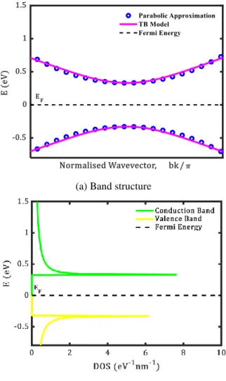
Fig. 2 shows the normalised band structure of PSi3NW.
From the band structure, a bandgap value is extracted, by computing the difference between CBM and VBM
𝐸𝑔= |𝐶𝐵𝑀 − 𝑉𝐵𝑀| (14)
The CBM and VBM extracted from the band structure of PSi3NW are 0.33 𝑒𝑉 and −0.33 𝑒𝑉 respectively. As a
result, the bandgap for PSi3NW is 0.66 𝑒𝑉.
This bandgap value is slightly higher from the previous research (𝐸𝑔= 0.58 𝑒𝑉) by Ding et al. (2013) because the
PSi3NW in this work is assumed as a perfect planar lattice
structure based on one-dimensional basis. Despite this slight deviation, the extracted bandgap energy is still suitable for the applications in the areas of nanoelectronics based on the standard value of bandgap, which between 0.4 𝑒𝑉 (Ni et al. 2014) and 3 𝑒𝑉 (Tang and Zhou 2013). The benchmark for band gap values are tabulated in Table 2.
Parabolic band assumption is applied around the CBM and VBM to obtain the effective mass for electrons and holes by fitting NNTB band structure. The obtained effective masses for electrons and holes are 𝑚𝑒∗ = 0.230𝑚0
and 𝑚ℎ∗ = 0.240𝑚0 , respectively where 𝑚0 is the
electron rest mass constant. Fig. 3(a) illustrates that the parabolic band structure around the CBM and VBM of PSi3NW is nicely fitted to the NNTB band structure. Fig.
3(b) shows the DOS plotted using Eqs. (6a) and (6b). From
Table 2 Benchmark of semiconductor bandgap values for nanoelectronics applications.
Materials Min. PSi3 Bulk Si Max.
Bandgap
(𝑒𝑉) 0.40 0.66 1.12 3.00
Fig. 2 Band diagram of PSi3NW in the zigzag direction
using NNTB model.
(a) Band structure
(b) DOS
Fig. 3 Band diagram and DOS of PSi3NW using
the DOS, it is shown that the peaks of DOS occur at the minimum point of conduction band and the maximum point of the valence band. The Fermi energy level 𝐸𝐹 is set to
zero in this work.
3.2 Carrier concentration of PSi3NW
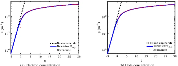
Figs. 4(a) and 4(b) show the intrinsic carrier concentrations of electrons and holes respectively for both the exact numerical FDI and reduced FDI calculations. From the graph, degenerate carrier concentration for electrons at 𝜂𝑐= 3 is extracted where 𝑛 = 1.739 × 10⁸ 𝑚−1 and for
holes 𝜂𝑣= 3 is 𝑝 = 1.786 × 10⁸ 𝑚−1. At the degenerate
regime, the electrons and holes concentrations start to saturate and do not have significant variations.
3.3 Intrinsic carrier velocity of PSi3NW
The intrinsic or thermal equilibrium velocities for electrons are computed and plotted. Fig. 5 shows the graph of intrinsic velocity for electrons versus temperature for three different electrons concentrations: 𝑛 = 1 × 10⁴ 𝑚−1
for non-degenerate regime, 𝑛 = 2 × 10⁸ 𝑚−1 and 𝑛 =
5 × 10⁸ 𝑚−1 for degenerate regime. From the results, the
relationship of intrinsic electrons velocity versus temperature is obtained: the intrinsic electrons velocity, 𝑣𝑖𝑒
is proportional to the temperature by 𝑇0.5.
As depicted in Fig. 6, the intrinsic velocity for electrons remains almost constant at non-degenerate regime where 𝑛 < 1 × 10⁸ 𝑚−1. Interestingly, it is observed that the
intrinsic electron velocity 𝑣𝑖𝑒 is increasing without
dependence on the temperature at the degenerate regime where 𝑛 > 1 × 10⁸ 𝑚−1 (which is clearly shown is the
dashed oval in Fig. 6). The intrinsic electrons velocity 𝑣𝑖𝑒
has become a simple function which merely depends on the electrons concentrations. This unique relationship (the independence of temperature at the degenerate regime) is consistent with the results in previous study involving 1D nanostructures (Ahmadi et al. 2009, Lim et al. 2018). Nevertheless, these findings are limited to devices within the ballistic transport regimes where the lengths of the devices are smaller than the MFP of the material.
Fig. 5 Electrons intrinsic velocity versus the temperature of PSi3NW for three different electrons concentrations.
Fig 6. Electrons intrinsic velocity versus the carrier concentration of PSi3NW at various temperature,
including ambient temperature, T = 300 K.
3.4 Current-voltage characteristics of PSi3NW
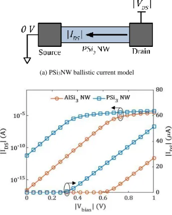
Fig. 7(b) compares the transfer characteristics of p-typedoped silicene using aluminium dopant atoms from
(a) Electron concentration (b) Hole concentration
(a) PSi3NW ballistic current model
(b) Transfer characteristics
Fig. 7 (a) Schematic diagram of I-V characteristic model; and (b) Comparison of I–V characteristics between PSi3NW of the proposed model and AlSi3NW adapted
from (Chuan, Wong et al. 2020c).
(Chuan et al. 2020c) and n-type doped silicene using phosphorus dopant atoms in this work. Under this ideal ballistic transport condition, both models have achieved the ideal subthreshold swing, 𝑆𝑆 = ∆𝑉𝑏𝑖𝑎𝑠/∆𝑙𝑜𝑔10𝐼 of
60 𝑚𝑉/𝑑𝑒𝑐 at room temperature, 𝑇 = 300 𝐾 . However, the threshold voltage, 𝑉𝑡ℎ1 obtained for PSi3NW is about
50% of the 𝑉𝑡ℎ2 obtained for AlSi3NW, where 𝑉𝑡ℎ1=
0.32 𝑉 and 𝑉𝑡ℎ2= 0.65 𝑉. In a practical MOSFET device,
these threshold voltages can be adjusted by tuning the work function of the gate metal and the source doping density. The results in Fig. 7(b) clearly show that the uniformly doped silicene could function as the channel materials for FET application. In future work, these nanostructures could be applied as the channels of FETs using transistor models such as the top-of-the-barrier nanotransistor model (Rahman et al. 2003, Chuan et al. 2020d, Chuan et al. 2021). Subsequently, the doped silicene could also be used for complementary metal-oxide-semiconductor (CMOS) technology, similar to previous studies on graphene (Banerjee et al. 2010, Goossens et al. 2017). The analytical equations computed in this work are useful for further device- and circuit-level modelling and simulations by creating SPICE models (Kazmierski et al. 2007).
4. Conclusion
In short, the proposed analytical model has achieved the
objectives of this work where the electronic and carrier transport properties of PSi3NW are computed. These
properties include the band structure, density of states (DOS), intrinsic carrier concentration, intrinsic carrier velocity and ballistic I-V characteristics. A bandgap value of 0.66 𝑒𝑉 is successfully opened originally semimetallic pristine silicene by using uniform substitutional doping with phosphorus. The extracted results include the degenerate electrons and holes concentrations of PSi3NW of 𝑛 =
1.739 × 10⁸ 𝑚−1 and 𝑝 = 1.786 × 10⁸ 𝑚−1 , respectively. In addition, it is observed the electrons intrinsic velocity is proportional to 𝑇0.5 at non-degenerate
regime and eventually becomes independent of temperature at degenerate regime. This work suggests that uniformly n-type doping is a viable technique to open semiconducting bandgap in silicene. As a result, the material can be applied for future nanoelectronics applications, especially in the digital switching devices. In summary, these findings provide insights for future research such as modelling and simulations of PSi3NW at the FET device and CMOS
circuit level.
Acknowledgements
The authors acknowledge the Research Management Centre (RMC) of Universiti Teknologi Malaysia (UTM) for providing excellent support and a stimulating research environment. Mu Wen would like to convey his gratitude for the award of PhD Zamalah Scholarship from the School of Graduate Studies, UTM. Michael Tan would like to acknowledge the financial support from UTM Fundamental Research (UTMFR) (Vote no.: Q.J130000.2551.21H51), which allowed the smooth progress of this research.
References
Ahmadi, M.T., Lau, H.H., Ismail, R. and Arora, V.K. (2009), “Current–voltage characteristics of a silicon nanowire transistor”, Microelectron. J., 40(3), 547-549. https://doi.org/10.1016/j.mejo.2008.06.060.
Ali, M., Pi, X., Liu, Y. and Yang, D. (2017), “Electronic and magnetic properties of graphene, silicene and germanene with varying vacancy concentration”, AIP Adv., 7(4), 045308. https://doi.org/10.1063/1.4980836.
Arora, V.K. (2015), Nanoelectronics: Quantum Engineering of Low-dimensional Nanoensembles, CRC Press, Florida, U.S.A. https://doi.org/10.1201/9781315222516.
Arora, V.K., Tan, M.L., Saad, I. and Ismail, R. (2007), “Ballistic quantum transport in a nanoscale metal-oxide-semiconductor field effect transistor”, Appl. Phys. Lett., 91(10), 103510. https://doi.org/10.1063/1.2780058.
Balendhran, S., Walia, S., Nili, H., Sriram, S. and Bhaskaran, M. (2015), “Elemental analogues of graphene: silicene, germanene, stanene, and phosphorene”, Small., 11(6), 640-652. https://doi.org/10.1002/smll.201402041.
Banerjee, S.K., Register, L.F., Tutuc, E., Basu, D., Kim, S., Reddy, D. and MacDonald, A.H. (2010), “Graphene for CMOS and beyond CMOS applications”, Proc. IEEE., 98(12), 2032-2046. https://doi.org/10.1109/JPROC.2010.2064151.
Bouadi, A., Bousahla, A.A., Houari, M.S.A., Heireche, H. and Tounsi, A. (2018), “A new nonlocal HSDT for analysis of
stability of single layer graphene sheet”, Adv. Nano Res., Int. J.,
6(2), 147. https://doi.org/10.12989/anr.2018.6.2.147.
Chhowalla, M., Jena, D. and Zhang, H. (2016), “Two-dimensional semiconductors for transistors”, Nature Rev. Mater., 1(11), 16052. https://doi.org/10.1038/natrevmats.2016.52.
Chuan, M., Wong, K., Hamzah, A., Rusli, S., Alias, N., Lim, C. and Tan, M. (2020a), “Two-dimensional modelling of uniformly doped silicene with aluminium and its electronic properties”, Adv. Nano Res., Int. J., 9(2), 105-112. http://doi.org/10.12989/anr.2020.9.2.105.
Chuan, M.W., Wong, K.L., Hamzah, A., Rusli, S., Alias, N.E., Lim, C.S. and Tan, M.L.P. (2020b), “2D honeycomb silicon: A review on theoretical advances for silicene field-effect transistors”, Curr. Nanosci., 16(4), 595-607. https://doi.org/10.2174/1573413715666190709120019. Chuan, M.W., Wong, K.L., Hamzah, A., Rusli, S., Alias, N.E.,
Lim, C.S. and Tan, M.L.P. (2020c), “Electronic properties and carrier transport properties of low-dimensional aluminium doped silicene nanostructure”, Physica E, 116 113731. https://doi.org/10.1016/j.physe.2019.113731.
Chuan, M.W., Wong, K.L., Hamzah, A., Rusli, S., Alias, N.E., Lim, C.S. and Tan, M.L.P. (2020d), “A review of the top of the barrier nanotransistor models for semiconductor nanomaterials”, Superlattice. Microst., 140 106429. https://doi.org/10.1016/j.spmi.2020.106429.
Chuan, M., Wong, K., Hamzah, A., Rusli, S., Alias, N., Lim, C. and Tan, M. (2021), “Device modelling and performance analysis of two-dimensional AlSi3 ballistic nanotransistor”, Adv. Nano Res., Int. J., 10(1), 91-99. http://doi.org/10.12989/anr.2021.10.1.091.
Datta, S. (1997), Electronic Transport in Mesoscopic Systems, Cambridge University Press, Cambridge, U.K. https://doi.org/10.1017/CBO9780511805776.
Datta, S. (2005), Quantum transport: Atom to transistor, Cambridge University Press, Cambridge, U.K. https://doi.org/10.1017/CBO9781139164313.
Ding, Y. and Ni, J. (2009), “Electronic structures of silicon nanoribbons”, Appl. Phys. Lett., 95(8), 083115. https://doi.org/10.1063/1.3211968.
Ding, Y. and Wang, Y. (2013), “Density functional theory study of the silicene-like SiX and XSi3 (X = B, C, N, Al, P) honeycomb lattices: The various buckled structures and versatile electronic properties”, J. Phys. Chem. C., 117(35), 18266-18278. https://doi.org/10.1021/jp407666m.
Gao, J., Zhang, J., Liu, H., Zhang, Q. and Zhao, J. (2013), “Structures, mobilities, electronic and magnetic properties of point defects in silicene”, Nanoscale, 5(20), 9785-9792. https://doi.org/10.1039/C3NR02826G.
Gert, A., Nestoklon, M. and Yassievich, I. (2015), “Band structure of silicene in the tight binding approximation”, J. Exp. Theo. Phys., 121(1), 115-121.
https://doi.org/10.1134/S1063776115060072.
Goossens, S., Navickaite, G., Monasterio, C., Gupta, S., Piqueras, J.J., Pérez, R., Burwell, G., Nikitskiy, I., Lasanta, T. and Galán, T. (2017), “Broadband image sensor array based on graphene– CMOS integration”, Nature Photonics, 11(6), 366-371. https://doi.org/10.1038/nphoton.2017.75.
Gupta, A., Sakthivel, T. and Seal, S. (2015), “Recent development in 2D materials beyond graphene”, Prog. Mater. Sci., 73, 44-126. https://doi.org/10.1016/j.pmatsci.2015.02.002.
Guzmán-Verri, G.G. and Lew Yan Voon, L.C. (2007), “Electronic structure of silicon-based nanostructures”, Phys. Rev. B., 76(7), 075131. https://doi.org/10.1103/PhysRevB.76.075131.
Harrison, W.A. (2004), Elementary Electronic Structure: Revised, World Scientific Publishing Company, Singapore. https://doi.org/10.1142/5432.
Huang, S., Kang, W. and Yang, L. (2013), “Electronic structure
and quasiparticle bandgap of silicene structures”, Appl. Phys. Lett., 102(13), 133106. https://doi.org/10.1063/1.4801309 IEEE (2018), International Roadmap for Devices and Systems
(IRDS). https://irds.ieee.org/.
Ismail, R., Ahmadi, M.T. and Anwar, S. (2016), Advanced Nanoelectronics, CRC Press, Florida, U.S.A. https://doi.org/10.1201/9781315217185.
Johari, Z., Ahmadi, M.T., Chek, D.C.Y., Amin, N.A. and Ismail, R. (2010), “Modelling of graphene nanoribbon Fermi energy”, J. Nanomater., 2010 14. https://doi.org/10.1155/2010/909347. Jooq, M.K.Q., Mir, A., Mirzakuchaki, S. and Farmani, A. (2018),
“Semi-analytical modeling of high performance nano-scale complementary logic gates utilizing ballistic carbon nanotube transistors”, Physica E, 104 286-296. https://doi.org/10.1016/j.physe.2018.08.008.
Kazmierski, T.J., Zhou, D. and Al-Hashimi, B.M. (2007). “A fast, numerical circuit-level model of carbon nanotube transistor”, 2007 IEEE International Symposium on Nanoscale Architectures.
https://doi.org/10.1109/NANOARCH.2007.4400855.
Kim, R. and Lundstrom, M. (2008), Notes on Fermi-Dirac Integrals, arXiv preprint arXiv:0811.0116. http://nanohub.org/resources/5475.
Le Lay, G., Solonenko, D. and Vogt, P. (2018), Synthesis of Silicene, Springer. https://doi.org/10.1007/978-3-319-99964-7_5.
Lew Yan Voon, L., Zhu, J. and Schwingenschlögl, U. (2016), “Silicene: Recent theoretical advances”, Appl. Phys. Rev., 3(4), 040802. https://doi.org/10.1063/1.4944631.
Lim, W.H., Hamzah, A., Ahmadi, M.T. and Ismail, R. (2017a), “Analytical study of the electronic properties of boron nitride nanosheet”, 2017 IEEE Regional Symposium on Micro and
Nanoelectronics (RSM).
https://doi.org/10.1109/RSM.2017.8069115.
Lim, W.H., Hamzah, A., Ahmadi, M.T. and Ismail, R. (2017b), “Band gap engineering of BC2N for nanoelectronic applications”, Superlattice. Microst., 112, 328-338. https://doi.org/10.1016/j.spmi.2017.09.040.
Lim, W.H., Hamzah, A., Ahmadi, M.T. and Ismail, R. (2018), “Performance analysis of one dimensional BC2N for nanoelectronics applications”, Physica E, 102, 33-38. https://doi.org/10.1016/j.physe.2018.04.005.
Lopez-Bezanilla, A. (2014), “Substitutional doping widens silicene gap”, J. Phys. Chem. C., 118(32), 18788-18792. https://doi.org/10.1021/jp5060809.
Lundstrom, M.S. and Antoniadis, D.A. (2014), “Compact models and the physics of nanoscale FETs”, IEEE T. Electron Dev.,
61(2), 225-233. https://doi.org/10.1109/TED.2013.2283253.
Lundstrom, M. and Jeong, C. (2013), Near-Equilibrium Transport: Fundamentals and Applications, World Scientific Publishing Company, Singapore. https://doi.org/10.1142/7975. Ma, L., Zhang, J.-M., Xu, K.-W. and Ji, V. (2014), “Nitrogen and
Boron substitutional doped zigzag silicene nanoribbons: Ab initio investigation”, Physica E, 60, 112-117. https://doi.org/10.1016/j.physe.2014.02.013.
Mohan, B., Kumar, A. and Ahluwalia, P.K. (2014), “Electronic and optical properties of silicene under uni-axial and bi-axial mechanical strains: A first principle study”, Physica E, 61, 40-47. https://doi.org/10.1016/j.physe.2014.03.013.
Molle, A., Grazianetti, C., Tao, L., Taneja, D., Alam, M.H. and Akinwande, D. (2018), “Silicene, silicene derivatives, and their device applications”, Chem. Soc. Rev., 47(16), 6370-6387. https://doi.org/10.1039/C8CS00338F.
Ni, Z., Zhong, H., Jiang, X., Quhe, R., Luo, G., Wang, Y., Ye, M., Yang, J., Shi, J. and Lu, J. (2014), “Tunable band gap and doping type in silicene by surface adsorption: towards tunneling transistors”, Nanoscale, 6(13), 7609-7618.
https://doi.org/10.1039/c4nr00028e.
Novoselov, K.S., Geim, A.K., Morozov, S.V., Jiang, D., Zhang, Y., Dubonos, S.V., Grigorieva, I.V. and Firsov, A.A. (2004), “Electric field effect in atomically thin carbon films”, Science,
306(5696), 666-669. https://doi.org/10.1126/science.1102896.
Rahman, A., Guo, J., Datta, S. and Lundstrom, M.S. (2003), “Theory of ballistic nanotransistors”, IEEE T. Electron Dev.,
50(9), 1853-1864. https://doi.org/10.1109/TED.2003.815366.
Schwierz, F., Pezoldt, J. and Granzner, R. (2015), “Two-dimensional materials and their prospects in transistor electronics”, Nanoscale, 7(18), 8261-8283. https://doi.org/10.1039/C5NR01052G.
Stpniak‐Dybala, A., Dyniec, P., Kopciuszyski, M., Zdyb, R., Jałochowski, M. and Krawiec, M. (2019), “Planar silicene: a new silicon allotrope epitaxially grown by segregation”, Adv. Funct. Mater., 29(50), 1906053. https://doi.org/10.1002/adfm.201906053.
Supriyo, D. (2017), Lessons From Nanoelectronics: A New Perspective On Transport -Part A: Basic Concepts, World Scientific Publishing Company, Singapore. https://doi.org/10.1142/10440-vol1.
Tang, Q. and Zhou, Z. (2013), “Graphene-analogous low-dimensional materials”, Prog. Mater. Sci., 58(8), 1244-1315. https://doi.org/10.1016/j.pmatsci.2013.04.003.
Tao, L., Cinquanta, E., Chiappe, D., Grazianetti, C., Fanciulli, M., Dubey, M., Molle, A. and Akinwande, D. (2015), “Silicene field-effect transistors operating at room temperature”, Nature
nanotechnol., 10(3), 227.
https://doi.org/10.1038/NNANO.2014.325.
Taur, Y., Mii, Y.-J., Frank, D.J., Wong, H.-S., Buchanan, D.A., Wind, S.J., Rishton, S.A., Sai-Halasz, G. and Nowak, E.J. (1995), “CMOS scaling into the 21st century: 0.1 μm and beyond”, IBM J. Res. Dev., 39(1.2), 245-260. https://doi.org/10.1147/rd.391.0245.
Vogt, P., De Padova, P., Quaresima, C., Avila, J., Frantzeskakis, E., Asensio, M.C., Resta, A., Ealet, B. and Le Lay, G. (2012), “Silicene: compelling experimental evidence for graphenelike two-dimensional silicon”, Phys. Rev. Lett., 108(15), 155501. https://doi.org/10.1103/PhysRevLett.108.155501.
Voon, L.L.Y., Lopez-Bezanilla, A., Wang, J., Zhang, Y. and Willatzen, M. (2015), “Effective Hamiltonians for phosphorene and silicene”, New J. Phys., 17(2), 025004. https://doi.org/10.1088/1367-2630/17/2/025004.
Wang, Z., Feng, T. and Ruan, X. (2015), “Thermal conductivity and spectral phonon properties of freestanding and supported silicene”, J. Appl. Phys., 117(8), 084317. https://doi.org/10.1063/1.4913600.
Wong, K.L., Chuan, M.W., Alias, N.E., Hamzah, A., Lim, C.S. and Tan, M.L.P. (2019), “Modeling of low-dimensional pristine and vacancy incorporated graphene nanoribbons using tight binding model and their electronic structures”, Adv. Nano Res., Int. J., 7(3), 209-221. http://doi.org/10.12989/anr.2019.7.3.209.