ICCAS2005 June 2-5, KINTEX, Gyeonggi-Do, Korea
1. INTRODUCTION
The SoC(System on a Chip) and digital technology development recently enable the emergence of high-performance and low-power image device, which is mainly adopted by various handheld devices like mobile phones and PDA. The CMOS(Complementary Metal-Oxide Semiconductor) image sensor is mainly used for such image devices. CMOS image sensor provides the better image sensing speed, smaller form-factor and lower power consumption than CCD(Charge Coupled Device) image sensor. In the past, CCD was preferred to CMOS because of its better image quality. However, CMOS has been more adopted recently because the improved semiconductor technology enables CMOS image quality to be much improved.
Compact Camera module(CCM) is widely used in PDA, mobile phone and PC web camera. With the greatly increasing use for internet and mobile applications, there has been a considerable demands for high speed production of CCM. The major burden of production of CCM are both assembly of lens module onto CMOS(Complementary Metal-Oxide Semiconductor) package and inspection of captured image quality of assembled CCM. In most assemble processes, CCMs are automatically assembled via surface mount technology. However, lens focus adjustment and the inspection of image of assembled CCM are executed by human operators. The inspection procedures by human operators are as follows. 1) lens focus adjustment, 2) 6 more imaging tests : black defect, dark defect, white balance test, color test, color temp test, dim test and so on. This several human operations take more 30secs for well skilled human operator to finish them. To reduce overall production time for CCM, we developed automatic inspection method for the inspection of CCM.
The developed inspection machine consists of image capture board , inspection chart with illumination system and imaging processing algorithm. We introduce development of a network based image capture board by using CMOS image sensor. The electrical chart is also developed to reduce taking time to change various inspection chart.
The performances of the developed inspection system and its algorithm are tested on samples of 10000 CCMs. The experimental results reveal that the proposed system can focus the lens of CCM within 5 secs and can recognize various types of defect of CCM modules with good accuracy and high speed.
2. CMOS IMAGE SENSOR AND IMAGE
CAPTURE BOARD
2.1 CMOS image sensor
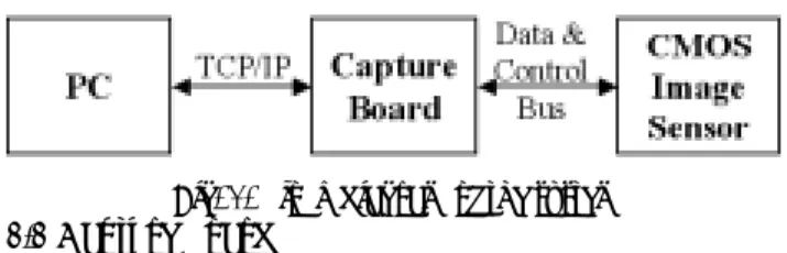
The target CMOS sensor is PO1030 CMOS image sensor made by Pixel Plus We develop network-based image capture board of this CMOS sensor. The size of sensor is 1/4.5 inches and has the color filter and micro lens. The output format supports 8bit YCbCr/YUV, 9bit Bayer Data, 5:6:5 RGB and 12bit 8:8:8 RGB. This supports two modes such as video mode and still image capture mode. The video mode displays the images continuously. The still image capture mode supports the mechanical and electrical shutter functions. The maximum frame rate is 30fps at 27MHz. By changing the internal register values, we could modify the image gains, balance, output formats and so on. The internal register value could be modified through I2C.[5]
Fig. 1. Block diagram of the system
2.2 Capture Board
The board consists of MPU(Micro Processing Unit), CPLD(Complex Programmable Logic Device) and CMOS image sensor. In addition, OS(Operating System) is used in order to control and develop the capture board more efficiently. Embedded Linux is used instead of Time OS and commercial embedded OS. Embedded Linux is open source and provides powerful networking and various hardware
Development of Automatic Visual Inspection for the Defect of
Compact Camera Module
Kuk Won Ko*, Yu Jin Lee*, Byung-Wook Choi and Johng-Hyung Kim
** * Deptment of Measurement and Control Engineering, Sunmoon University, Asan Chungnam, Korea(Tel : +82-41-530-2348; E-mail: [email protected])
**School of Mechanical Design & Automation Engineering, Seoul Nat’l Univ. of Tech., Seoul, Korea (Tel : +82-2-970-6357; E-mail: [email protected])
Abstract:
Compact Camera Module(CCM) is widely used in PDA, Celluar phone and PC web camera. With the greatly increasing use for mobile applications, there has been a considerable demands for high speed production of CCM. The major burden of production of CCM is assembly of lens module onto CCD or CMOS packaged circuit board. After module is assembled, the CCM is inspected. In this paper, we developed the image capture board for CCM and the imaging processing algorithm to inspect the defects in captured image of assembled CCMs. The performances of the developed inspection system and its algorithm are tested on samples of 10000 CCMs. Experimental results reveal that the proposed system can focus the lens of CCM within 5s and we can recognize various types of defect of CCM modules with good accuracy and high speed.Keywords: Compact Camera Module, Automatic Visual Inspection
ICCAS2005 June 2-5, KINTEX, Gyeonggi-Do, Korea
architectures. Additionally, the various application programs, development tools and libraries, which are provided free, enable the reduced development time and cost.[2,3,4], CPLD is implemented by using VHDL(Very high speed integrated circuit Hardware Description Language), in order to store the image data from CMOS image sensor into the RAM. The Linux-based application program, which enables image data stored in RAM to be transferred to PC by using TCP/IP, is also developed. This program consists of I2C communication, GPIO(General Purpose I/O) handling and network socket programs. The Fig.1 shows the system block diagram. The ARM7TDMI based S3C4530A SoC is used in the board, in order to transmit the image data from CMOS image sensor through TCP/IP. This integrates the Ethernet controller as an MPU for network-based system. And it include I2C interface [6] . CPLD is used to store image data from CMOS image sensor into RAM. In this CPLD, counter, buffer and comparator are programmed in VHDL, correspond to the output format of CMOS image sensor. S3C4530A include peripheral like RJ-45 port for networking, Ethernet driver, serial port for debugging, connectors between CMOS image sensor and capture board and so on. The system memory includes the flash memory storing kernel and file system including user application, SDRAM running Linux and SRAM storing the image data from CMOS image sensor. Fig 2 shows a layout and interface between MPU and CMOS image sensor.
Fig. 2(a). System layout of the capture board
Fig. 2(b). Interface between capture board and CMOS image sensor
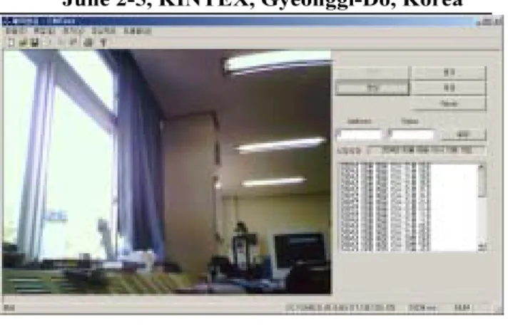
Fig. 3. The applied viewer program
2.3 Image capture program and viewer program
The image capture program stores image data into SRAM and transmits the stored image data to PC through TCP/IP, controlling the CMOS image sensor. This program runs on uClinux and is developed on Linux environment by using a cross complier and library. As a TCP/IP socket server, this includes the function of controlling I2C and GPIO, in order to control the CMOS image sensor. This program is activated while Linux is being booted. Once it is activated, it waits for connection with the client. When it is connected, initialize the CMOS image sensor, sets up the register value of CMOS image sensor and captures and sends an image to the client according to commanders from the client. Viewer program is the one to display the image data sent from capture board. As a network socket client, viewer program sends the commander of controlling CMOS image sensor to a capture board and display the bitmap after changing YCbCr format data from the board to RGB format data.
3.. IMAGE PROCESSING ALGORITHM
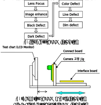
In this chapter, we introduce the developed image processing algorithm to inspect the defect of captured image of assembled CCM and also corresponding inspection charts for each defect. To detect various defects, several charts should be used. To reduce the time to change charts, the inspect chart electrically is shown via LCD monitor. Figure 4 shows the overall imaging inspection procedures for CCM. The each defect and its inspection algorithm are explained.
3.1. Focus and resolution inspection algorithm
The lens of CCM should be well focused to acquire a good quality images. A chart image for focus inspection is shown in Fig 5(a). The image processing algorithm for focus inspection is based on the sharpness of edge. The well-focused image has sharp edge as shown in Fig 5(b). The sharpness of edge is calculated by the variance of data set which can be extracted by the gray level difference of adjacent pixel through horizontal line as shown in Fig 5(d). After assembling lens unit onto CMOS cell, the lens is unfocused and mostly is fully loosened. The focusing unit rotates lens body and make lens focused At every step, the edge sharpness is calculated and the rotation angle which has minimum value is the best focused lens angle . Fig. 5(e) is the plot of variance in real lens focusing procedure.
3.2. Image enhancement algorithm
After the procedure of inspection for lens focus of CCM is well finished, the acquired image is shown in Fig. 6(a). Although the imager is well focused, the image is slightly
ICCAS2005 June 2-5, KINTEX, Gyeonggi-Do, Korea
distorted in brightness. The pixels in corner image are slightly darker than those in center because of lens characteristics. This distortion of brightness in image arises difficulties in image process to extract the defect from acquired image. The multi-layered neural network is used to calibrate the brightness in image. Fig.(b) is the inverse model for bright calibrated image and fig. 6(c) show fully calibrated image.
Lens Focus Black Defect Dark Defect Line Defect Dim defect Color Defect Image enhance Lens Focus Black Defect Dark Defect Line Defect Dim defect Color Defect Image enhance
(a) flowchart of CCM inspection Test chart (LCD Monitor)
Interface board Camera 고정 Jig Connect board Test chart (LCD Monitor)
Test chart (LCD Monitor)
Interface board Interface board Camera 고정 Jig Camera 고정 Jig Connect board Connect board
(b) schematics of CCM module inspection Fig. 4. Flowchart of overall CCM inspection
3.3 Dark/bright dot defect inspection algorithm
Dark dot defect is caused by the defect of CMOS pixel which is bright or visible and can be always be seen on an all black background. Bright dot defect is caused by the defect of CMOS pixel which is dark and can be always be seen on an all white background. These pixels on CMOS are damaged or do not work correctly.
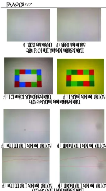
To detect dark dot defect, the background should be black or dark, the inspection chart for the dark dot defect should be black. Otherwise, to detect bright detect, the background should be white, the inspection chart for the bright dot defect should be white or bright. Fig. 7(a) and (b) show the charts for dark/bright dot defect respectively. And, Fig (c) and (d) show the each defect image. The defect can be easily separated from background by simple thresholding method.
3.4 Line Dot defect inspection algorithm
Line dot defect is caused by the defect of two adjacent CMOS pixel which is always the same color vertically or always of different color dots horizontally as shown in Fig 8(a) and (b). The each R,G and B pixel in image are projected vertically and horizontally. The defect line has different value in projected pixel data and can be easily detected by simple threshold method.
3.5 Color inspection algorithm
Fig. 9(a) shows a color inspection chart which consists of red, green and blue. The each color R,G and B pixel value of acquired image is compared to known R,G and B pixel value. The color defect has pixels which can not be read color correctly and the color defected pixel has greatly different value. Fig. 9(b) shows the image of color defect.
3.6 Dim Defect inspection algorithm
Dim defect is caused by dust on the lens. Fig. 10(a) and (b) are images of dim defect. The dusts or particles on lens
make blurred dark area on images and the size of particle is unknown. This is called dim and it is very difficult to detect because the graylevel difference between adjancet pixels is very small. Fig .10(c) shows the graylevel profile on dim defect.. The self-organizing neural network is used to memorize this defected profile. The neural network memorizes profiles of this defect and distinguish this defect from image after training procedure.
(a) focus chart (b) well focused (c) defocused
A B
A B
sharp edge
unsharp
edge sharp edge unsharp edge
Horizontally 1st derivative pixel data
A B
A B
sharp edge
unsharp
edge sharp edge unsharp edge
A B
A B
sharp edge
unsharp
edge sharp edge unsharp edge
Horizontally 1st derivative pixel data
(d) edge sharpness
rotation angle(x30 degree)
v a r i a n c e best focus
rotation angle(x30 degree)
v a r i a n c e best focus
(e) lens rotation angle vs variance at focusing step. Fig. 5. Focus inspection algorithm
(a) distorted brightness (b) inverse model (c) calibrated image Fig. 6. Image enhancement algorithm
(a) chart for dark dot detect (b) defect of dark dotted image
(c) chart for black dot detect (d) defect of black dotted image
Fig. 7. Dark dot defect inspection
ICCAS2005 June 2-5, KINTEX, Gyeonggi-Do, Korea
(a) line detect(pink) (b) line detect(blue) Fig. 8. Dark dot defect inspection
(a) chart of color inspection (b) color defected image Fig. 9 Color detect inspection
(a) small dim defected image (b) large dim defected image
(c) small dim defected image (d) large dim defected image Fig. 10 Dim defect inspection
4. EXPERIMENTS AND DISCUSSIONS
To evaluate the performance of the proposed method, a series of experiments was performed for 2500 samples. The experimental equipments for CCM is shown in Fig. 11. Table 1 shows the inspection results. For 2500 sample, black /dark/line/color defect is perfectly detected, and there are only 2 error in focus stage because lens bodies do not work correctly. However, the success rate of dim inspection is 98.2% success rate. The large particle on the lens can be detected with a good accuracy, but the particle within 2-3 pixel size can not be easily detected because the graylevel difference between adjacent pixel is nearly 3-4 graylevel value. To detect this small dim defect, we should develop new method to detect this small dim defect. The total inspection time is 29s to execute all inspection procedures include loading and unloading CCM and the processing time is only 8s.
Table 1. Inspection results
Inspection Focus Black/
Dark
Color Line Dim
Success 2498 2500 2500 2500 2455
Fail 2 0 0 0 45
Success
rate 99.92% 100% 100% 100% 98.2%
5. Conclusions
In this paper, an automated vision system and vision algorithms for compact camera module has been developed. The developed electric chart and image enhancement algorithm reduce the subsequent image processing algorithm to calibrate bright distortion and to reduce the time to change each chart for several inspections. As a result, simple image processing algorithms such as a binary threshold method, a simple edge extracting method, and pixel valve comparison method are easily implemented. The experimental results show the developed vision system can detect the defect of CCM with a good accuracy and fast processing time less than 30secs of human operators in real CCM production line.
LCD chart
focusing unit LCD chart
focusing unit
Fig. 11 Vision system for inspection of CCM.
ACKNOWLEDGMENTS
This work is supported by Kormi Corporation and RRC in Sunmoon university and conducted through 2005.
REFERENCES
[1] A.Filippov, “Reconfigurable High Resolution Network Camera”, Proc,11th Annual IEEE Symp, on Field-Programmable Custom Computing Machines, 2003
[2] A. Lennon, “Embedded Linux”, IEE Review, pp33-37, May 2001
[3] S.Hong, “Embedded Linux Outlock in the Post Industry”, Proc. 6th Int. Symp. On Object-Oriented Real-Time Distributed Computing, 2003
[4] A.Filippov, “Using Embedded Linux in a reconfigurable high-res network camera”, LinuxDevices, www.linuxdevices.com, 2003
[5] PO1030 Data Sheet, Pixelplus, 2003 [6] S3C4530A User’s guide, Samsung 2001 [7] http://uclinux.org/description
[8] Paul Cheng-Hsin Liu, Abnay Trivedi, “Machine vision processing/selection in printed circuit board manufacturing”, IEEE trans.
[9] G. Burel, F. Bernard and W.J. Venema, “Vision feedback for SMD placement using neural network”, IEEE international conference, pp 1491-1496,-1995.
[10] D. H. Ballard, "Computer Vision", Prentice Hall, 1985. [11] Juyang Weng, Paul Cohen and Marc Herniou, " Camera
Calibration with Distortion Models and Accuracy Evalution", IEEE Trans, on Pattern Analysis and Machine Intelligence, Vol. 14, No. 10, October 1992 [12] Codourey, A., "Dynamic modeling and mass matrix
evaluation of the DELTA parallel robot for axes decoupling control," Proceedings of the 1996 IEEE/RSJ
International Conference on Intelligent Robots and Systems, Vol. 3, pp.1211 - 1218, 1996