In-Ga-Zn-O semiconductors using
microwave and e-beam radiation, and the
associated thin film transistor properties
Cite as: AIP Advances 9, 025204 (2019); https://doi.org/10.1063/1.5082862
Submitted: 25 November 2018 . Accepted: 30 January 2019 . Published Online: 11 February 2019 Seong Cheol Jang, Jozeph Park, Hyoung-Do Kim, Hyunmin Hong, Kwun-Bum Chung, Yong Joo Kim, and Hyun-Suk Kim
ARTICLES YOU MAY BE INTERESTED IN
Control of O-H bonds at a-IGZO/SiO2 interface by long time thermal annealing for highly
stable oxide TFT
AIP Advances
7, 125110 (2017);
https://doi.org/10.1063/1.5008435
Ultra-wide bandgap amorphous oxide semiconductors for NBIS-free thin-film transistors
APL Materials
7, 022501 (2019);
https://doi.org/10.1063/1.5053762
Metal oxide semiconductor thin-film transistors for flexible electronics
Low temperature activation of amorphous
In-Ga-Zn-O semiconductors using microwave
and e-beam radiation, and the associated
thin film transistor properties
Cite as: AIP Advances 9, 025204 (2019);doi: 10.1063/1.5082862 Submitted: 25 November 2018 • Accepted: 30 January 2019 • Published Online: 11 February 2019Seong Cheol Jang,1,a)Jozeph Park,2,a)Hyoung-Do Kim,1Hyunmin Hong,3Kwun-Bum Chung,3,b)Yong Joo Kim,4,c)
and Hyun-Suk Kim1,d)
AFFILIATIONS
1Department of Materials Science and Engineering, Chungnam National University, Daejeon 34134, Republic of Korea 2Department of Materials Science and Engineering, Korea Advanced Institute of Science and Technology, Daejeon 34141,
Republic of Korea
3Division of Physics and Semiconductor Science, Dongguk University, Seoul 04620, South Korea 4Biosystems Machinery Engineering, Chungnam National University, Daejeon 34134, Republic of Korea a)Contributions: These authors contributed equally to this work
b)corresponding authors:kbchung@dongguk;edu; c)corresponding authors:[email protected] d)corresponding authors:[email protected]
ABSTRACT
In-Ga-Zn-O (IGZO) films deposited by sputtering process generally require thermal annealing above 300◦C to achieve satisfac-tory semiconductor properties. In this work, microwave and e-beam radiation are adopted at room temperature as alternative activation methods. Thin film transistors (TFTs) based on IGZO semiconductors that have been subjected to microwave and e-beam processes exhibit electrical properties similar to those of thermally annealed devices. However spectroscopic ellipsom-etry analyses indicate that e-beam radiation may have caused structural damage in IGZO, thus compromising the device stability under bias stress.
© 2019 Author(s). All article content, except where otherwise noted, is licensed under a Creative Commons Attribution (CC BY) license
(http://creativecommons.org/licenses/by/4.0/).https://doi.org/10.1063/1.5082862
Amorphous silicon (a-Si) has been the most commonly used semiconductor material for thin film transistors (TFTs) in the field of flat panel displays for the past many decades. How-ever, its field effect mobility is limited to less than 1 cm2/Vs, and stability can be a problem in some applications.1
Amor-phous oxide semiconductors (AOSs) have attracted consid-erable attention as possible substitutes owing to their high carrier mobility and areal uniformity.2–4 The oxide
semi-conductor material that is already available in the market is amorphous In-Ga-Zn-O (a-IGZO), which is implemented in TFT backplanes of liquid crystal displays (LCDs) or organic light emitting diode (OLED) panels.5,6Devices based
on IGZO semiconductor exhibit relatively high field-effect mobility (>10 cm2/Vs) compared to their a-Si counterparts.7
To deposit a-IGZO, magnetron sputtering is commonly used. However, the fabrication of IGZO TFTs with reasonably good electrical performance usually requires thermal annealing at temperatures near 300◦C.8,9 Many research group aim at
decreasing the annealing temperature to enable the fabrica-tion of devices on plastic substrates, so that flexible displays may be realized in a cost effective way.10–12
In this work, microwave and electron beam (e-beam) radi-ation methods are adopted to reduce the treatment tem-perature for the activation of IGZO TFTs. It is shown that
reasonable TFT performance may be obtained by both meth-ods, however e-beam annealing appears to cause structural damage in the IGZO layers, resulting in devices that are more susceptible to degradation upon bias stress.
IGZO TFTs with an inverted staggered bottom gate struc-ture were fabricated on highly doped p-type Si substrates with thermally grown 100 nm-thick SiO2 layers. The highly doped p-type Si and 100 nm SiO2were used as the gate elec-trode and gate insulator, respectively. 30 nm-thick IGZO films were deposited by radio frequency (RF) magnetron sputtering using a 3-inch IGZO target with an atomic composition ratio of In:Ga:Zn = 1:1:1. The plasma gas used was Ar, at a flow rate of 20 sccm. The working pressure was maintained at 7 mTorr and an RF power of 100 W was applied to the IGZO target. After performing the annealing treatment on the IGZO film, a 150-nm thick indium tin oxide (ITO) film was deposited and patterned to form the source/drain electrodes, using shadow masks. The channel width and length of the IGZO devices were 800 and 200 µm, respectively.
The microwave annealing of IGZO layers was performed at a power and frequency of 600 W and 2.45 GHz, respectively. Microwave radiation was applied for 1 hour in air ambient. In general, ZnO-based materials can absorb the electromagnetic wave energy in frequency range of 2 to 18 GHz.13Therefore,
it is anticipated that IGZO will absorb the microwave energy at the frequency applied in this work. For e-beam anneal-ing, an electron beam with an energy and current of 0.2 MeV and 10 mA, respectively. Here the duration was varied from 3 to 10 minutes in air. Additionally, a reference IGZO TFT with a typical thermal annealing process was fabricated for com-parison. The thermal annealing was conducted in a conven-tional rapid thermal annealing system in air ambient for 1 hour at 300◦C.
The crystal structures of the IGZO films were examined by grazing incidence angle X-ray diffraction (XRD; Rigaku, D/MAX2500, Cu Kα radiation). The diffraction patterns of the samples were taken in the 2θ range from 20 to 80◦ with a step size of 0.05◦. The chemical bonding states were exam-ined using X-ray photoelectron spectroscopy (XPS) using a monochromatic Mg Kα (1253.6 eV) source and a pass energy of 50 eV.
The electrical characteristics of TFTs were evaluated in the dark at room temperature using an HP 4156B semicon-ductor parameter analyzer, under air ambient conditions. The field-effect mobility was extracted in the saturation regime with the drain voltage (VD) fixed at 10 V. The devices were subjected to negative bias stress (NBS), positive bias stress (PBS) and negative bias illumination stress (NBIS). For NBS and NBIS, the gate voltage (VG) and drain voltage (VD) applied were -20 and 0.1 V, respectively. A light source with a luminance of 1500 lux was used to illuminate the devices from the top dur-ing NBIS. For PBS, the applied VGand VDwere 20 and 0.1 V, respectively. Each stress test was conducted in air at room temperature for 1 hr.
The transfer characteristics of IGZO films are shown in Figure 1. Table I consists of representative parameters such as saturation filed effect mobility (µsat), threshold volt-age (Vth) and subthreshold swing (SS). Metallic behavior was
FIG. 1. Representative transfer characteristics of the IGZO TFTs with the active
layer subjected to different annealing processes.
observed in the pristine TFTs fabricated without annealing, which implies that a relatively high carrier concentration is present in the IGZO layer. Semiconducting properties could be obtained after thermal, microwave, and e-beam treatment. Thermally annealed IGZO TFTs exhibit µsat, Vth, and SS val-ues of 8.10 cm2/Vs, -1.34 V and 0.32 V/decade, respectively. Increased field effect mobility (11.3 cm2/Vs) is observed in devices fabricated with microwave annealed IGZO, accom-panied with a slight negative shift of the initial Vth value (-1.54 V). Devices that have been exposed to 3 min e-beam annealing exhibit relatively low mobility (7.40 cm2/Vs) with slightly negative Vth(-1.95 V) values. As the e-beam annealing time is increased to 10 minutes, extremely low performance is obtained, as shown inFigure 1.
TABLE I. Device parameters of the IGZO TFTs, including theµsat, S.S., Vth, and Ion/Ioffratio values, with respect to different annealing processes.
Annealing Type µsat(cm2/Vs) S.S (V/dec) Vth(V) Ion/Ioff
Pristine N/A
Thermal 8.10 0.24 -1.34 109
Microwave 11.25 0.32 -1.54 109 e-beam 3min 7.40 0.60 -1.95 109
TABLE II. ∆ Vthvalues under NBS, PBS, NBIS, for the IGZO TFTs with respect to different annealing processes.
Annealing Type Thermal Microwave e-beam NBS ∆Vth(V) −0.38 −0.57 −1.08 PBS ∆Vth(V) 0.6 0.54 0.99 NBIS ∆Vth(V) −0.1 −0.3 −6.86
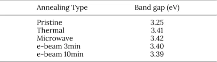
FIG. 2. Grazing incidence angle X-ray diffraction (GIAXRD) patterns of IGZO TFTs
with respect to different annealing processes.
To evaluate the stability of IGZO TFTs, negative bias stress (NBS), positive bias stress (PBS), and negative bias illumina-tion stress (NBIS) tests were conducted on three samples, each having been subjected to thermal, microwave, and 3-min e-beam annealing. The results are summarized in Table II. As the stress time increases, all IGZO TFTs undergo negative (NBS, NBIS) and positive (PBS) shifts in Vth. While the devices fabricated with microwave and thermal annealing undergo relatively small shifts in threshold voltage (|Vth| < 1 V) under all stress conditions, those having been subjected to e-beam annealing exhibit rather poor stability with ∆Vth values of -1.08, 0.99, and -6.86 V under NBS, PBS, and NBIS, respec-tively. At this point it may be anticipated that a high concen-tration of defects acting as charge traps is present in the IGZO film exposed to e-beam radiation.
X-ray diffraction (XRD) and atomic force microscopy (AFM) analyses were carried out to examine the microstruc-ture of the IGZO films annealed under different conditions. Figure 2shows the diffraction patterns of each type of IGZO films appear to be amorphous regardless of the annealing pro-cess. This indicates that both microwave and e-beam radi-ation used in the present study do not crystallize the IGZO films. The AFM surface topography images are shown in Figure 3. Compared with the pristine IGZO film (0.12 nm), the surface roughness increases with thermal annealing (0.28 nm). Microwave annealed IGZO has a lower root mean square (RMS) roughness value (0.19 nm) than those of e-beam annealed IGZO layers (0.44 and 0.83 nm for 3-min and 10-min e-beam radiation, respectively). The above results imply that as the thermal budget increases, the surface roughness increases, and may be indicative of the overall defect density in the IGZO film.
XPS analyses were performed to analyze the chemical bonding states of oxygen anions in the annealed IGZO layers. Figure 4shows the O 1s peak spectra of each film. Peaks were
FIG. 3. Atomic force microscope
topog-raphy images of IGZO films with respect to different annealing processes.
FIG. 4. XPS O 1s spectra of IGZO films
with respect to different annealing pro-cesses.
resolved as the sum of three sub-peaks, centered at 530.7 eV (O1), 531.4 eV (O2), and 532.5 eV(O3). The sub-peak O1 is related to oxygen ions forming metal-oxide bonds, while peak O2 originates from oxygen anions near oxygen vacant sites, and peak O3 is related to hydroxyl groups in the IGZO films.14 In
oxide semiconductors, oxygen deficiency is strongly related to the generation of free carriers,15therefore sub-peak O2 is
generally used to estimate the concentration of oxygen related defects and free carriers. All annealing processes result in decreased sub-peak O2 area, which is indicative of decreas-ing free carrier density, thus inducdecreas-ing relatively positive initial Vthvalues.
Figure 5(a) shows the refractive indices (R-value) as a function of photon energy, extracted from spectroscopic ellipsometry (SE), which may reflect the structural density of the films. Generally, dense layers exhibit relatively high R-values.16,17 Compared to the pristine IGZO, the samples
that have been subjected to thermal and microwave annealing exhibit higher R-values over the entire photon energy range (1 to 5 eV). On the other hand, e-beam annealing appears to reduce the R-values considerably. This suggests that the rel-atively rapid e-beam treatment induces structural modifica-tions within the IGZO layer, while the time for rearrangement is not sufficient.Figure 5(b)shows the extinction coefficients, also extracted from the SE spectra. The optical band gap
values can be extrapolated using the Tauc method, as shown in the equation below:18
(αhν)1/2= A(hν − E
g)
where h is Planck constant, ν the photon frequency, α the absorption coefficient, Eg the band gap, and A a propor-tionality constant. The band gap values are summarized in Table III. All annealing processes result in increased optical bandgap.
Figure 5(c) shows the band edge states below the con-duction band minimum of each IGZO films, extracted from the imaginary dielectric functions. The fitted Gaussian peaks rep-resent unoccupied trap states within the forbidden gap. The band edge state below the conduction band may be resolved into a shallow band edge state (D1) and a deep band edge state (D2), which are located at 3.18 and 2.56 eV from the valence band maximum, respectively. Shallow band edge states are related to the free carrier concentration, while deep band states reflect the amount of defects that act as traps of scat-tering centers.19In oxide semiconductor, the carrier mobility
is generally proportional to the free carrier concentration.20
In addition, trapping or scattering of carriers are most likely to be associated with the degradation of TFT devices under bias stress. The sub-area peak ratios of the D1 and D2 states are summarized in Figure 5(d). The number of shallow band
FIG. 5. (a) Index of refraction and (b)
extinction coefficient and (c) enlarge-ment of band edge states below the conduction band minima of the IGZO films with respect to different annealing processes, measured by spectroscopic ellipsometry (SE). (d) Relative sub-peak areas of the D1 and D2 states in IGZO, with respect to the different annealing processes.
edge states (D1) appears to decrease under all annealing pro-cesses compared to the pristine IGZO, resulting in positive shifts in the initial Vthin the associated TFTs. The relative area of D1 states is smallest after 10 min e-beam annealing, which indeed results in the poorest TFT performance. Microwave and 3 min e-beam annealing have similar D1 sub-peak area, however the D2 portion is larger in the latter, which may account for the more pronounced degradation of the corre-sponding TFT under bias stress. Here the D2 states are antic-ipated to act as charge traps, thus causing relatively large Vthshifts upon prolonged bias stress. Such defects are highly likely to be generated by the physical energy of the e-beam, which may induce structural damage within the IGZO layers. It is therefore necessary to optimize a balance between the total thermal budget and physical damage induced in the semicon-ductor, in order to lower the process temperature for the fabrication of IGZO TFTs. Here, microwave annealed devices exhibit the best performance and stability, owing to the con-version of microwave energy into thermal energy without causing structural damage.
In the present study, effects of microwave and e-beam annealing on IGZO films and their corresponding TFTs have been investigated. The IGZO TFTs fabricated by microwave
TABLE III. Optical band gap values of IGZO films with respect to different annealing processes, extracted using the Tauc method.
Annealing Type Band gap (eV)
Pristine 3.25
Thermal 3.41
Microwave 3.42
e-beam 3min 3.40
e-beam 10min 3.39
annealing exhibit a typical field effect mobility of 11.3 cm2/Vs and a threshold voltage of -1.54 V. The devices subjected to e-beam annealing exhibit a slightly lower mobility of 7.40 cm2/Vs and a more negative threshold voltage of -1.95 V. Both annealing processes activate the IGZO active layer suc-cessfully at room temperature. As a reference, it is shown that thermally annealed IGZO TFTs exhibit µsat and Vth values of 8.10 cm2/Vs and -1.34 V, respectively. IGZO TFTs fabricated by thermal and microwave annealing exhibit good performance and stability throughout NBS, PBS, NBIS. On the other hand, while similar performance may be obtained by e-beam anneal-ing, the stability appears to be compromised, especially in the presence of light (NBIS). Thin film analyses suggest that structural damage is induced during e-beam radiation, which generate electrical defect levels within the forbidden bandgap of IGZO. The latter are manifested as band edge states in the spectroscopic ellipsometry results.
This work was supported by Basic Science Research Pro-gram through the National Research Foundation of Korea (NRF) funded by the Ministry of Education (Grant No: NRF-2017R1D1A1B03032375) and also by the MOTIE (Ministry of Trade, Industry & Energy (Grant No: 10051403)) and KDRC (Korea Display Research Corporation) support program for the development of future devices technology for display industry.
The authors declare no competing financial interest. REFERENCES
1Y. Ye, R. Lim, and J. M. White, “High mobility amorphous zinc oxynitride
semiconductor material for thin film transistors,”J. Appl. Phys.106, 074512
(2009).
2K. Nomura, H. Ohta, A. Takagi, T. Kamiya, M. Hirano, and H. Hosono,
“Room-temperature fabrication of transparent flexible thin-film transistors using amorphous oxide semiconductors,”Nature432, 488–492 (2004).
3A. Nathan, S. Lee, S. Jeon, and J. Robertson, “Amorphous oxide
semi-conductor TFTs for displays and imaging,”J. Display Technol.10, 917–927
(2014).
4H. Hosono, “Ionic amorphous oxide semiconductors: Material design,
car-rier transport, and device application,”J. Non-Crys. Solids352, 851–858
(2006).
5J. H. Lee, D. H. Kim, D. J. Yang, S. Y. Hong, K. S. Yoon, P. S. Hong, C. O. Jeong,
H. S. Park, S. Y. Kim, S. K. Lim, S. S. Kim, K. S. Son, T. S. Kim, J. Y. Kwon, and S. Y. Lee, “World’s largest (15-inch) XGA AMLCD panel using IGZO oxide TFT,”SID Int. Symp. Dig. Tech. Pap.39, 625−628 (2008).
6J. K. Jeong, J. H. Jeong, J. H. Choi, J. S. Im, S. H. Kim, H. W. Yang, K. N. Kang,
K. S. Kim, T. K. Ahn, H. J. Chung, M. Kim, B. S. Gu, J. S. Park, Y. G. Mo, H. D. Kim, and H. K. Chung, “12.1-inch WXGA AMOLED display driven by indium-gallium-zinc oxide TFTs array,”SID Int. Symp. Dig. Tech. Pap.39,
1–4 (2008).
7C. C. Lo and T. E. Hsieh, “Preparation of IGZO sputtering target and
its applications to thin-film transistor devices,”Ceram. Int.38, 3977–3983
(2012).
8Y. J. Tak, B. D. Ahn, S. P. Park, S. J. Kim, A. R. Song, K. B. Chung, and H. J.
Kim, “Activation of sputter-processed indium–gallium–zinc oxide films by simultaneous ultraviolet and thermal treatments,” Sci Rep 6, 21869
(2016).
9D. G. Yang, H. D. Kim, J. H. Kim, K. Park, J. H. Kim, Y. J. Kim, J. Park, and H. S.
Kim, “Performance and stability of amorphous In-Ga-Zn-O thin film tran-sistors involving gate insulators synthesized at low temperatures,”J. Alloy. Compd.729, 1195–1200 (2017).
10H. Lee, K. S. Chang, Y. J. Tak, T. S. Jung, J. W. Park, W. G. Kim, J. Chung, C. B.
Jeong, and H. J. Kim, “Electric field-aided selective activation for indium-gallium-zinc-oxide thin film transistors,”Sci Rep6, 35044 (2016).
11Y. J. Tak, S. P. Park, T. S. Jung, H. Lee, W. G. Kim, J. W. Park, and H. J.
Kim, “Reduction of activation temperature at 150◦
C for IGZO films with
improved electrical performance via UV-thermal treatment,”J. Inf. Disp.17,
73–78 (2016).
12M. G. Stanford, J. H. Noh, K. Mahady, A. V. levlev, P. Maksymovych, O. S.
Ovchinnikova, and P. D. Rack, “Room temperature activation of InGaZnO thin-film transistors via He+irradiation,”ACS Appl. Mater. Inter.9, 35125–
35132 (2017).
13L. F. Teng, P. T. Liu, Y. J. Lo, and Y. J. Lee, “Effects of microwave
anneal-ing on electrical enhancement of amorphous oxide semiconductor thin film transistor,”Appl. Phys. Lett.101, 132901 (2012).
14J. H. Park, Y. Kim, S. Yoon, S. Hong, and H. J. Kim, “Simple method to
enhance positive bias stress stability of In−Ga−Zn−O thin-film transistors using a vertically graded oxygen-vacancy active layer,”ACS Appl. Mater. Interfaces6, 21363–21368 (2014).
15J. S. Park, W. J. Maeng, H. S. Kim, and J. S. Park, “Review of recent
devel-opments in amorphous oxide semiconductor thin-film transistor devices,”
Thin Solid Films520, 1679–1693 (2012).
16K. Sangwal and W. Kucharczyk, “Relationship between density and
refrac-tive index of inorganic solids,”J. Phys. D20, 522 (1987).
17J. H. Kim, C. O. Chung, D. Sheen, Y. S. Sohn, H. C. Sohn, J. W. Kim,
and S. W. Park, “Effect of fluorine incorporation on silicon dioxide pre-pared by high density plasma chemical vapor deposition with SiH4/O2/NF3
chemistry,”J. Appl. Phys.96, 1435 (2004).
18V. M. Bhuse, P. P. Hankare, K. M. Garadkar, and A. S. KHomane, “A simple,
convenient, low temperature route to grow polycrystalline copper selenide thin films,”Mater. Chem. Phys.80, 82–88 (2003).
19H. W. Park, A. Song, S. Kwon, D. Choi, Y. Kim, B. H. Jun, H. K. Kim, and
K. B. Chung, “Enhancing the performance of tungsten doped InZnO thin film transistors via sequential ambient annealing,”Appl. Phys. Lett.112, 123501
(2018).
20J. Y. Kwon, D. J. Lee, and K. B. Kim, “Transparent amorphous oxide