25-3 / H. J. Yun
• IMID 2009 DIGEST
Abstract
We have fabricated pentacene based organic thin film transistors (OTFTs) with formulated poly[4-vinylphenol] (PVP) gate dielectrics. The gate dielectrics is composed of PVP, poly[melamine-co-formaldehyde] (PMF) and photo-initiator [1-phenyl-2-hydroxy-2-methylpropane-1-one, Darocur1173]. By adding small amount (1 %) of photo-initiator, the cross-linking temperature is lowered to 115 ℃, which is lower than general thermal curing reaction temperature of cross-linked PVP (> 180 ℃). The hysteresis and the leakage current of the OTFTs are also decreased by adding the PMF and the photo-initiator in PVP gate dielectrics.
1. Introduction
OTFTs are of great interest because it is studied for low cost, low-temperature, large area electronic applications such as smart card, radio frequency identification (RFID) tags, and flat panel displays (FPD).1-2 An important criterion in the fabrication of
organic TFTs is the choice of the gate dielectric material. Among the polymer dielectrics reported to date, one of the most useful material is cross-linked PVP, which has good dielectric properties and high carrier mobility. Although the resulting cross-linked PVP material possesses excellent chemical resistance and good dielectric performance, the high temperature for the thermal cross-linking reaction makes this material unsuitable for common low-cost plastic substrates.3-4 Hysteresis of drain current (ID)-gate
voltage (VG) curves and the threshold voltage (VT)
shift are another serious problems to be solved. In this work, we have investigated the electrical properties of the PVP gate dielectrics cross-linked at
lower temperature (115 ℃) by adding a photo-initiator and a poly[melamine-co-formaldehyde] (PMF). The leakage current of metal-insulator-metal (MIM) capacitors and the hysteresis of pentacene TFTs with photo-cured PVP gate dielectrics were also studied. Pentacene TFTs were fabricated on glass substrates.
2. Experimental
The electrical insulator properties of the Co-PVP were measured by MIM structure. Glass substrates were cleaned with acetone, isopropyl alcohol (IPA) and deionized (D. I.) water for 10 minutes, respectively. Then, the cleaned glass baked on the hotplate performed at 120 °C for dry. Aluminum (Al) gate electrode was thermally evaporated onto the cleaned glass substrate with a shadow mask. For the polymer dielectrics, the PVP dielectric layer was obtained from a poly[4-vinylphenol] (PVP) precursor (10 wt %), poly[melamine-co-formaldehyde] (PMF) (2 wt %), and a photo-initiator [1-phenyl-2-hydroxy-2-methylpropane-1-one, Darocur1173] (0 ~ 9 wt %) in a propylene glycol monomethyl ether acetate (PGMEA) solvent. The insulator layer of Co-PVP was spin-coated and exposed to 254 nm UV irradiation (17.1 mW cm-2) for 15 minute to catalyze the cross-linking reaction. These films were hardened through baking at 115℃ for an additional 90 sec.
Figure 1 shows a schematic view of a bottom contact (BC) pentacene TFT used in the present work. A 30 nm thick pentacene active layer was deposited by thermal evaporation under base pressure of 5×10⁻⁷
torr. In order to get well ordering pentacene film, the deposition rate was controlled with 2 steps as follows; the deposition rate of 0.3 Å/min was maintained for
Organic Thin Film Transistors with Cross-linked PVP Gate
Dielectrics by Using Photo-initiator and PMF
Ho-jin Yun
1,2, Kyu-Ha Baek
1, Kun-sik Park
1, , Hong-sik Shin
1,
Yong-hyun Ham
1, Ga-Won Lee
2, Kijun Lee
2, Jinsuk Wang
2, and Lee-Mi Do
11Electronics and Telecommunications Research Institute (ETRI), 138 Gajeongno, Yuseong-gu, Daejeon, 305-700, Korea
TEL:82-42-860-5235, e-mail: [email protected] 2Chungnam National University, Daejeon, 305-764, Korea
25-3 / H. J. Yun
IMID 2009 DIGEST •
the first 30 Å and the other 270 Å thick penetacene was deposited with relatively high deposition ratio of 0.3 Å/sec. Finally, silver source/drain electrodes were deposited by the thermal evaporation; giving TFTs with a channel length of 0.1 mm and a channel width of 2 mm.
3. Results and discussion
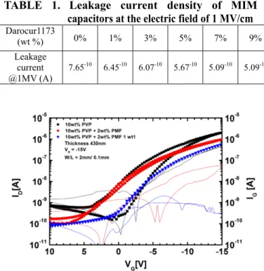
We measured the leakage current of the PVP dielectrics to evaluate the dielectric characteristics of the MIM capacitors with the cross-linked PVP films. As shown in Fig. 2, the leakage current decreased as increasing the content of Darocur1173 from 0 to 9 wt %. Table 1 summarizes the leakage current of MIM capacitors at the electric field of 1 MV/cm. The hysteresis of ID-VG curves of the pentacene TFTs was
remarkably reduced by adding a PMF, and an addition of small amount (1%) of photo-initiator (Darocur 1173) further reduced the hysteresis as shown in Fig. 3. The down-shift of the VT when VG is reversely swept
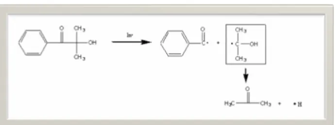
is normally caused by the presence of mobile charge in the gate dielectrics, and we think the mobile charges are removed by cross-linking reaction. Other electrical parameters such as carrier mobility, threshold voltage, subthreshold swing, and on/off current ratio of the BC pentacene TFTs were extracted and summarized in Table 2. The leakage current and hysteresis were sharply decreased in case of adding a initiator. It is determined that because a photo-initiator makes the type in which itself does with the molecule series(decomposition) and it forms radical into the Hydrogen donor and complex like figure 4, it comes with the Leakage current and the hysteresis is decreased.
Fig. 1. Schematic cross-sectional view of organic thin film transistor
Fig. 2. Leakage current density of MIM capacitors with PVP dielectric films cross-linked by various content of Darocur1173 (0 to 9 wt %).
TABLE 1. Leakage current density of MIM
capacitors at the electric field of 1 MV/cm Darocur1173 (wt %) 0% 1% 3% 5% 7% 9% Leakage current @1MV (A) 7.65-10 6.45-10 6.07-10 5.67-10 5.09-10 5.09-10
Fig. 3. Electrical transfer characteristics of BC pentacene TFTs with cross-linked PVP gate dielectrics.
TABLE 2. Electrical properties of BC pentacene TFTs with cross-linked PVP gate dielectrics
25-3 / H. J. Yun
• IMID 2009 DIGEST
Fig. 4. The reaction schematic diagram of the photoinitiator (Darocur1173).
4. Summary
The hysteresis and the leakage current of the OTFTs are decreased by adding the PMF and the photo-initiator in PVP gate dielectrics. We here demonstrate the viability of using polymer gate dielectric for OTFTs, where the low temperature and good electrical property can potentially facilitate the integration of organic thin-film transistor circuits on plastic substrates.
5. Acknowledgements
This research was supported by the Ministry of Knowledge Economic (Grant No.10031791) and convergence research program funded by Korea Research Council for Industrial Science and Technology.
5. References
1. M. Leufgen, A. Lebib, T. Muck, U. Bass, V. Wagner, T. Borzenko, G. Schmidt, J. Geurts, and L. W. Molenkamp, Appl. Phys. Lett. 84, p.1582 (2004). 2. F. M. Li, A. Nathan, Y. Wu, and B. S. Ong, Appl.
Phys. Lett. 90, p. 133514 (2007)
3. F. Y.Yang, K. J. Chang, M. Y. Hsu and C. C Liu, Chem, p. 5927 (2008)
4. Y. L. Loo et al., Commercialization of Organic Electronics, MRS BULLETIN, Vol 33, No.7 (2008)