44-3 /M. kimura
IMID 2009 DIGEST •
Abstract
Sensor applications of thin-film transistors (TFTs), such as photosensor, magnetic sensor, temperature sensor and chemical sensor, are introduced. Active-matrix circuits and amplifying circuits using poly-Si TFTs are integrated with these sensors to improve sensor performances and generate additional functions. These sensors may be promising applications after flat-panel displays (FPDs) in giant-micro electronics.
1. Introduction
Thin-film transistors (TFTs), such as amorphous-Si TFTs1 and poly-Si TFTs2, have been widely used for flat-panel displays (FPDs)3-5, such as home televisions, computer monitors, mobile displays and electronic papers. However, TFTs have general advantages, such as large area, flexible substrate and low cost. Not only FPDs but also other applications must be potential candidates to utilize these advantages6.
In this presentation, sensor applications of TFTs,
Sensor Applications of Thin-Film Transistors
Photosensor, Magnetic Sensor, Temperature Sensor and Chemical Sensor
-Mutsumi Kimura
1, Yuta Miura
1, Takeshi Ogura
1, Tomohisa Hachida
2,
Yoshitaka Nishizaki
2, Takehiko Yamashita
2, Takehiro Shima
1, Hayami Hashimoto
1,
Yohei Yamaguchi
1, Masaaki Hirako
1, Toshifumi Yamaoka
1, Satoshi Tani
1,
Yoshiki Imuro
1, Kosuke Bundo
1, Yuki Sagawa
2, Koushi Setsu
11Dept. of Electronics and Informatics, Ryukoku University, Seta, Otsu 520-2194, Japan TEL:81-77-543-5111, e-mail: [email protected]
2Graduate School of Materials Science, Nara Institute of Science and Technology, Takayama, Ikoma 630-0192, Japan
Keywords : Thin-film transistor, Photosensor, Magnetic sensor, Temperature sensor, Chemical sensor
Retina array Vdd Vbias Vout Vadjust Retina pixel TFPT C u rr ent m irro r Load re s is tanc e Iphoto Imirror 1 2 3 4 5 6 7 8 9 1 1 2 3 4 5 6 7 8 9 1 1 2 3 4 5 6 7 8 9 1 1 2 3 4 5 6 7 8 9 1 White Red Green Blue 0 1 2 3 4 Vout 5(V) (b) Artificial retina Fig. 1. Photosensor. 0 100 200 300 -1 0 1 2 3 4 5 6 Ip h o to ( p A ) Vapply (V) Lphoto=1000lx White Red Green Blue Vapply Iphoto Lphoto p i n Cathode Anode Cathode Anode 50nm Ctrl 75nm Vctrl W/L=100/10um Vctrl=2V
44-3 /M. kimura
• IMID 2009 DIGEST
such as photosensor, magnetic sensor, temperature sensor and chemical sensor, will be introduced7. Active-matrix circuits and amplifying circuits using poly-Si TFTs are integrated with these sensors to improve sensor performances and generate additional functions. These sensors may be promising applications after FPDs in giant-micro electronics.
2. Photosensor
Photosensors using TFTs8 are key devices for ambient-light sensors9, image scanners10, artificial retinas11, etc. We propose p/i/n thin-film photototransistors (TFPT). Figure 1(a) shows the device structure of the p/i/n TFPT and its device characteristic, dependence of the photo-induced current (Iphoto) on the applied voltage (Vapply) and illuminating color when the control voltage (Vctrl) and photo illuminance (Lphoto) are fixed. It is found that the p/i/n TFPT has large sensitivity difference between the illuminating colors. It is due to the photon energy and absorption coefficient of the poly-Si12.
Moreover, we propose artificial retinas using p/i/n TFPTs. It is advantageous that they can be fabricated on transparent and flexible substrates, which is suitable to implant it into human eyeballs. Figure 1(b) shows the device structure of the artificial retina, array arrangement and pixel circuit, and its device characteristic, profile of the output voltage (Vout) when the pinhole pattern is projected. The current mirror to amplify Iphoto and load resistance to convert it to Vout are integrated in the pixel circuit using poly-Si TFTs. It is found that the profile of Vout is correct in spite of the sensitivity difference between the illuminating colors. It is due to the amplifying
function of the pixel circuit.
3. Magnetic sensor
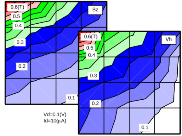
We propose micro Hall devices using poly-Si thin-films13. It is advantageous that the area profile and real-time behavior of the magnetic field can be observed. Figure 2(a) shows the device structure of the micro Hall device and its device characteristic, dependence of the Hall voltage (Vh) on the magnetic flux density (Bz). It is found that Vh can be proportional to Bz even by micro Hall devices as fine as 50 µm.
Figure 2(b) shows the profile of Bz measured by Gauss meter and micro Hall device. It is found that the profile of Bz can be correctly observed by the micro Hall device. We will integrate the active-matrix circuits and Vh amplifying circuits using poly-Si TFTs in the future.
4. Temperature sensor
We propose temperature sensors using poly-Si TFTs. It is because the transistor characteristics are strongly dependent on the device temperature. It is advantageous that the area profile and real-time behavior of the local temperature can be observed. Figure 3(a) shows the I-V characteristic of the poly-Si TFT in variation of the device temperature (T).
Figure 3(b) shows the dependence of Ids on T in variation of Vgs. It is found that Ids can be strongly dependent on T. In particular, in the case that the logarithmic change is required, Ids in the off-region and sub-threshold region is available. On the other hand, in the case that the linear change is required, Ids in the on-region is available. We will integrate the
0 10 20 30 40 50 0 0.5 1 Bz (T) Vh ( u V) Vd=0.1(V) Id=10(µA) Bz 10µm Id VH Vd 1 2 3 4 51 2 3 4 5 1 2 3 4 5 Bz 0.6(T) Vd=0.1(V) Id=10(µA) Vh 0.5 0.4 0.3 0.2 0.1 0.6(T) 0.5 0.4 0.3 0.2 0.1
(a) micro Hall device (b) Area profile
44-3 /M. kimura
IMID 2009 DIGEST •
active-matrix circuits and T-signal amplifying circuits using poly-Si TFTs in the future.
5. Chemical sensor
Chemical sensors using thin-film devices are also interesting for gas sensors14, deoxyribonucleic acid (DNA) sensors15, etc. We propose integrated potentiostats with electrochemical cell16. It is advantageous that they can be integrated on a glass wafer in order to assemble with micro-total analysis systems (µ-TASs). Figure 4(a) shows the device structure of the integrated potentiostats with electrochemical cell, microscope photograph and equivalent circuit. The integrated potentiostat consists of three operational amplifiers fabricated by poly-Si TFTs, and the electrochemical cell consists of three electrodes fabricated by printing technology.
Figure 4(b) shows the cyclic-voltammetry measurement using the integrated potentiostats with electrochemical cell, amperometric enzymatic-redox reaction using glucose oxidase and ferrocene mediator. It is found that the fundamental characteristic can be confirmed, the glucose concentration of 0.7 mM is detected and the integrated potentiostat has sufficient sensitivity in detection of glucose concentration for some medical application such as diabetic diagnosis.
7. Acknowledgements
The authors thank Drs. Tokihiro Yoshikawa, and Tomohiro Tadokoro of NEC Schott Components, Drs. Hiroyuki Hara, Hitoshi Fukushima, Hiroshi Takiguchi, Shinobu Yokokawa, Hiroshi Maeda, Simon W.-B. Tam, Toshihiko Yokoyama, Tomoyuki Kamakura, Satoshi Inoue, Frontier Device Research Center, and Device Development Support Department of Seiko Epson, Drs. Shin Koide, Yutaka Kobashi, and Tomoyuki Ito of Epson Imaging Devices, Prof. Eiichi Tamiya of Osaka University, Prof. Yuzuru Takamura of JAIST, Prof. Takashi Kakiuchi of Kyoto University, Dr. Tsuneo Munakata of Jedat, and Drs. Yoichi Suzuki,
Syogo Ishikawa, and Hiromitsu Umezawa of FDK.
This research is partially supported by collaborative research with Seiko Epson, Joint Research Center for Science and Technology at Ryukoku University, High-Tech Research Center Program from MEXT, research facility equipment from MEXT, special research facilities from Ryukoku University, and internship program with NEC Schott Components.
8. References
1. Y. Kuo, Thin Film Transistors, Materials and Processes, 1: Amorphous Silicon Thin Film Transistors, Kluwer Aademic Publishers, Boston (2004).
2. Y. Kuo, Thin Film Transistors, Materials and Processes, 2: Polycrystalline Silicon Thin Film Transistors, Kluwer Aademic Publishers, Boston (2004).
3. J.-H. Lee, S.-T. Wu and D. Liu, Introduction to Flat Panel Displays, John Wiley & Sons, New York (2009).
4. M. Kimura, I. Yudasaka, S. Kanbe, H. Kobayashi, H. Kiguchi, S. Seki, S. Miyashita, T. Shimoda, T. Ozawa, K. Kitawada, T. Nakazawa, W. Miyazawa and H. Ohshima, IEEE Trans. Electron Devices, 46 [12], 2282 (1999).
5. http://www.sony.jp/products/Consumer/oel
6. M. Kimura and T. Shima, AM-FPD '06 Digest of Technical Papers, p. 73 (2006).
7. M. Kimura, T. Hachida, Y. Nishizaki, T. Yamashita, T. Shima, T. Ogura, Y. Miura, H. Hashimoto, M. Hirako, T. Yamaoka, S.
1E-13 1E-12 1E-11 1E-10 1E-9 1E-8 1E-7 1E-6 1E-5 1E-4 1E-3 0 50 100 150 200 T (℃) Id s ( A ) 0 1 2 3 Vgs=-5∼-4 4∼10 0 10 20 30 40 50 0 50 100 150 200 T (℃) Id s ( u A ) 1 2 3 4 Vgs=-5∼0 5 (b) Temperature dependence Fig. 3. Temperature sensor.
1E-13 1E-12 1E-11 1E-10 1E-9 1E-8 1E-7 1E-6 1E-5 1E-4 1E-3 -5 0 5 10 Vgs (V) Id s ( A ) n-type LDD tsi/tox=50/75nm W/L=400/4.5µm Vds=0.1V T=20°C 50 100 200
44-3 /M. kimura
• IMID 2009 DIGEST
Tani, Y. Yamaguchi, Y. Sagawa, K. Setsu, Y. Imuro, K. Bundo,
T. Yoshikawa and T. Tadokoro, IDMC⋅3DSA⋅Asia Display '09
Proceedings, Tue-S06-01 (2009)
8. T. Yamashita, T. Shima, Y. Nishizaki, M. Kimura, H. Hara and S. Inoue, Jpn. J. Appl. Phys., 47 [3], 1924 (2008).
9. S. Koide, S. Fujita, T. Ito, S. Fujikawa and T. Matsumoto, IDW '06 Proceedings, p. 689 (2006).
10. T. Nishibe and H. Nakamura, AM-FPD '06 Digest of Technical Papers, p. 61 (2006).
11. M. Kimura, T. Shima, T. Yamashita, Y. Nishizaki, H. Hara and S. Inoue, J. SID, 16 [6], 661 (2008).
12. T. Hachida, T. Ogura, Y. Miura, Y. Nishizaki, T. Yamashita, T. Shima and M. Kimura, AM-FPD '09 Proceedings, p. 141 (2009)
13. M. Hirako, T. Yamaoka, S. Yani and M. Kimura, JSAP ’08 Spring Meeting Extended Abstracts, p. 891 (2008).
14. L. Mariucci, A. Pecora, C. Puglia, C. Reita, G. Petrocco and G. Fortunato, Jpn. J. Appl. Phys., 29 [12], L2357 (1990).
15. P. Estrela, A. G. Stewart, P. Migliorato and H. Maeda, IEDM ’04 Technical Digest, p. 1009 (2004).
16. M. Kimura, H. Fukushima, Y. Sagawa, K. Setsu, H. Hara and S. Inoue, IEEE Trans. Electron Devices, 56 [9] (1999) to be published. Integrated potentiostat Electrochemical cell Op -a m p 1 Op -a m p 2 Op -a m p 3 Ra Rb Rc Counter Reference Work
I-V converter V controller 3 electrodes Potentiostat Counter Reference Work Vra / Vrb Ra Vin -+ Rb -+ Op-amp 1 Op-amp 2 - + Op-amp 3 Vrc Vout Rc Counter Reference Work V controller I-V converter
3 electrodes
(a) Integrated potentiostat with electrochemical cell