P1-35 / M. S. Kim
IMID 2009 DIGEST •
Abstract
The LCD based on Kerr effect is highly interesting because it uses an optically isotropic state with no need of alignment layer and it shows sub-millisecond response time. The problem of the device is that it requires very high operating voltage and the transmittance is relatively low compared with other LCDs that use nematic LC. In this work, we study on various electrode structures and driving method which can lower operating voltage.
1. Introduction
Recently, blue phases have become interested issue in area of liquid crystal displays (LCDs). Liquid crystal molecules of nematic phase have been being utilized in almost all range of LCDs. However, the nematic phase has intrinsic weak points basically, firstly alignment layer treatment, secondly intrinsic viewing angle dependence, thirdly insufficient slow response time for high quality moving pictures. As a solution, optically isotropic-anisotropic changing liquid crystal composites such as polymer-stabilized blue phase liquid crystalline (BP LC) or optically isotropic-nano structured liquid crystal composite have been an issue because of its optically isotropic state from its cubic lattice and fast response time from its high elastic constant [1-4].
Conventional polymer-stabilized BP LC devices have been driven by in-plane electric field with inter-digital shaped electrodes in order to switch isotropic
state (voltage-off) to anisotropic state (voltage-on) along the induced birefringence of BP LC via the Kerr effect [5-6]. However it needs high operating voltage according to previous reports [7-9].
In the BP LC devices, the interdigitated electrodes are only on a bottom substrate with thickness of less than 1 ㎛ so that electric fields are formed between electrodes only near the bottom substrate. In other words, the intensity of electric fields is not strong enough to induce the birefringence up to whole area of the cell, and in addition, the intensity of electric field is proportional to the length between electrodes. To reduce the operating voltage, electric fields should be utilized intensively and to intensify the electric field, length between electrodes should be reduced. For a narrow electrode gap, there should be many numbers of electrodes for a pixel size over 100 µm, which will decrease transmittance because no transmittance is generated above electrodes due to no in-plane field. This means the transmittance and the operating voltage are in trade-off relation.
To overcome such high operating voltage and low transmittance problems, wall-shaped electrode was proposed [10]. In the ideal case of the condition, the electrode height should be as much as higher than cell gap to form more electric fields. However, it is not an easy process to have electrode wall over few µm. In the real situation, the electrode should be topped on organic film or resin such like column spacer. Hence real electrode height can be up to 3~4 µm.
Reduction of an Operating Voltage of Liquid Crystal
Display based on Kerr Effect
Min Su Kim, Miyoung Kim, Byeong Gyun Kang, Mi-Kyung Kim, Sukin
Yoon, Suk-Won Choi
1, Gi-Dong Lee
2, and Seung Hee Lee
Dept. of Polymer Nano Science and Technology, Chonbuk National University, Chonju, Chonbuk, 561-756, Korea
Tel.:+82-63-270-2343, E-mail: [email protected]
1Dept. of Display Materials Engineering and Materials Research Center for Information Displays, Kyung Hee University, Korea,
2Dept. of Electronics, Dong-A University, Korea
P1-35 / M. S. Kim
• IMID 2009 DIGEST
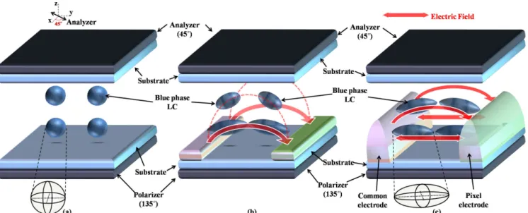
Figure 1. (a) Optically isotropic state at voltage off state in BP LC, (b) Voltage-on state BP LC in conventional in-plane electric field driving electrode structure, (c) Voltage-on state BP LC in proposed elliptic-like shaped electrode structure.
In this paper, we studied on reduction of the operating voltage by utilizing well-occupied electric fields with proposed electrodes. Besides, for optimal structure of the proposed electrode, we simulated the variation of the distance between electrodes with driving by two transistors [11].
In the voltage-off state, the BP LC is in optically isotropic state from its cubic lattice so that it shows dark under crossed polarizers as shown in Figure 1 (a). In the voltage-on state, the birefringence is induced along the electric fields (E) and its magnitude is determined by equation;
∆ninduced = λKE2 (1)
where ∆ninduced is the induced birefringence, λ is the
wavelength of an incident light, and K is the Kerr constant of the BP LC composites [5-6]. The large K and strong E are very important to enhance ∆ninduced,
so that we focused on the factor E to induce more. The cell is composed of crossed polarizers and BP LC driven by in-plane electric fields, therefore the normalized transmittance (T) of the device associated with the phase retardation can be described as follows;
T= sin2 2ψ×sin2(πd∆n
induced(V)/ λ) (2)
where ψ is an angle between one of the transmission axes of the crossed polarizers and the LC director, and
d is LC layer thickness with induced birefringence. In
order to maximize the transmittance, ψ should be equal to 45o and d∆n
induced should be λ/2.
2. Electrode structure designed in in-plane
electric field device
In order to improve transmittance, the electrode structure with enough distance between pixel and common electrode is preferred. To simulate the device for optimal condition, we have employed 3-dimensional commercial simulation software Techwiz (Sanayi, Korea). In the in-plane electric field devices, we have chosen w and l to be 4µm and 6µm, respectively and the Kerr constant of the mixture is 1.0ⅹ10-9m/V2 in the device. The in-plane electric field is always generated between electrodes so that
Figure 2. Voltage dependent transmittance curves in conventional electrode, and elliptic electrode with height of 1µm, 2µm and 3µm.
P1-35 / M. S. Kim
IMID 2009 DIGEST • Figure 3. Comparison of electric fields intensity between (a) conventional in-plane electric field driving electrode structure, (b) proposed elliptic-like shaped electrode structure and (c) principle of single transistor driving, (d) principle of two transistors driving.
the region with transmittance can be 6µm out of 10µm (= w + l). It explains the transmitted area in the in-plane electric field driven cell is about 60%.In conventional in-plane electric field devices, the electrodes thickness is just approximately less than 1µm high in real situation. Therefore, in-plane field which induces birefringence of BP LC exists only between electrodes, that is, no transmittance occurs above electrodes. In addition, intensity of in-plane electric fields is dependent on vertical direction such that it is getting weaken as far away from electrode substrate. Consequently, the ∆n induced is dependent on
the vertical position, as illustrated in Figure 1 (b). To induce more birefringence not only between electrodes but also above electrodes, the electric field should be formed intensively up to the vertical position. Unlike conventional LCDs, the optically isotropic-anisotropic liquid crystal composite devices do not require alignment layer treatment, so that the height or shape of the electrodes would not degrade the dark state quality of the BP LC devices. In an ideal condition of the electrode is rectangular shape with height as high as cell gap to form the electric fields in whole area of the cell. However, in real situation, the electrode with such as indium tin oxide (ITO) cannot be stacked as much as more than 1µm. So, such as organic film or insulator should be patterned on the bottom substrate firstly and then deposit ITO and patterned it. As a result, electrode structure can be elliptic-like, so that the electric fields are formed intensively along the height of the electrode vertically, as shown in Figure 1 (c). More retardation can be
induced from optically isotropic BP LC layer from the proposed structure.
Figure 2 shows the voltage dependent transmittance curves according to its electrode height. As above mentioned, the cell with electrode structure 3 µm high shows the lower operating voltage (76V) than that of conventional electrode (132V) by up to 57.6 % with slightly improved transmittance.
3. Reduction of the operating voltage
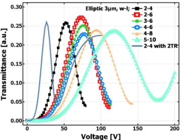
Figure 3 shows comparison of equi-potential lines between the conventional in-plane electric field driving electrode structure, and the proposed elliptic-like shaped electrode structure. As clearly can be seen, stronger in-plane field between electrodes is formed compared to that of the conventional structure. Even though the proposed electrode structure reduces operating voltage of the BP LC, the operating voltage is still high to drive the device due to the low Kerr constant. Another way of lowering operating voltage is to use two transistors [11], as can be seen in Fig. 3(d).Figure 4 shows voltage dependent transmittance curves according to the w, l in w-l = 2-4, 2-6, 3-6, 4-6, 4-8, 5-10, 2-4 µm with two transistors with fixed elliptic-like shaped electrode height 3 µm. Basically, reducing w contributes to more transmittance because the transmitted area can be promoted, increasing l contributes to more transmittance under fixed w because the transmitted area can be promoted also and
P1-35 / M. S. Kim
• IMID 2009 DIGEST
Figure 4. Voltage dependant transmittance curves in 3µm height elliptic-like shaped electrode according to the electrode width (w) and the distance between electrodes (l) in w-l ; 2-4, 2-6, 3-6, 4-6, 4-8, 5-10, 2-4 µm
with two transistors.
intensity of the electric field contributes to less operating voltage in the condition such as less length of l because if the applied voltage is fixed, less l contributes to more electric field intensity. Distinguishing the curves by w=l/2 length which are 2-4, 3-6, 4-8, 5-10, the short length of l contributes to lower operating voltage from intensive electric field and to occur more transmittance from reducing the length of w. Comparing the case of 2-4 and 2-6, the length of l is promoted under the length of fixed w so that the transmittance is increased and the operating voltage is heightened from weakened electric field. We can approach same rationale in to the case of 3-6 and 4-6, 4-6 and 4-8, as well. Finally, the operating voltage of 2-4 is 52V and in the case of 2-4 with two transistors is 26V. Apparently, the operating voltage is reduced by half of the single transistor driving with two transistors driving. As a result, the operating voltage is lowered up to 19.7% (26V) by using elliptic-like shaped electrode and two transistors from the operating voltage of the conventional device, 132V.
4. Conclusion
We have proposed new device structure for LCDs based on Kerr effect. The device with elliptic-like shaped electrodes and two transistors lowers driving voltage and improves transmittance. The results contribute greatly to improve electro-optic characteristics of next generation LCDs based on Kerr effect.
Acknowledgements
This work was supported by WCU project.
5. References
1. H. Kikuchi, M. Yokota, Y. Hisakado, H. Yang, T. Kajiyama, Nat. Mater. 1, pp64-68 (2002).
2. Heinz-S. Kitzerow, Chem. Phys. Chem. 7, pp63-66 (2006).
3. S. W. choi, S. Yamamoto, Y. Haseba, H. Higuchi, H. Kikuchi, App. Phy. Lett, 92, p043119 (2008). 4. S. Yokoyama, S. Mashiko, H. Kikuchi, K. Uchida,
and T. Nagamura, Adv. Mater. 18, pp48-51 (2006). 5. Y. Hisakado, H. Kikuchi, T. Nagamura, and T.
Kajiyama, Adv. Mater. 17, pp96-98 (2005).
6. Y. Haseba, H. Kikuchi, T. Nagamura, and T. Kajiyama, Adv. Mater. 17, pp2311-2315 (2005). 7. H. Kikuchi, H. higuchi, Y. Haseba, and T. Iwata,
SID Symposium Digest 38, pp1737-1740 (2007).
8. Y. Haseba, H. Kikuchi, J. Soc. Info. Display 14, pp551-556 (2006).
9. Z. Ge, S. Gauza, M. Jiao, H. Xianyu, and S. T. Wu,
Appl. Phys. Lett. 94, p101104 (2009).
10. M. S. Kim, M. Kim, J. H. Jung, K. S. Ha, S. Yoon, E. G. Song, A. K. Srivastava, S. W. Choi, G. D. Lee and S. H. Lee, SID Symposium Digest 15, pp1615-1618 (2009).
11. J. H. Jung, J. W. Park, M. Kim, Y. J. Lim, T. J. Chung, and S. H. Lee, Proc. IDRC, pp158–160, (2008).