2-3 / T. Yano
• IMID 2009 DIGEST
Abstract
PDP panels with MgO protective layer are manufactured by using the “all-in-vacuum” process we have established [1]. This is the process aiming to keep the MgO surface as clean as possible after the evaporation. The panels are evaluated in term of discharge voltage, aging time, luminance, luminous efficacy, discharge time-lag. It is confirmed that the “all-in-vacuum” process particularly improves the aging time, discharge voltage and the discharge time-lag.
1. Introduction
It was reported that the discharge characteristics, such as a dynamic voltage margin, a firing voltage, and a statistical address delay time, of the MgO-PDP manufactured by using vacuum sealing method could be improved [2,3].
Now, we are developing the “all-in-vacuum” manufacturing system. By using our system, we can manufacture the panel without air exposure of MgO layer after evaporation. By keeping the MgO surface in vacuum, MgO surface could be kept clean. By sealing the panel in vacuum, MgO surface could be kept clean and the impurities in the discharge gas in the panel decrease. Therefore, our method is applicable to the PDPs with high γ but reactive
protective materials such as CaO and SrO.
In this work, we manufacture the panel without air exposure of MgO layer after evaporation by using our “all-in-vacuum” system, and evaluate the discharge characteristics of the panel.
2. Experimental
The advantage of PDP manufacturing method under the vacuum condition was evaluated on 4-inch test panel, where the X and Y electrode of the front panel was a stripe with 180 µm in width, and inter-electrode
distance between the X and Y electrode is 80 µ. Rib
structure of the real panel is also a stripe with 130 µm
in height.
Figure 1 shows the flowchart of conventional and “all-in-vacuum” process. The difference of conventional and “all-in-vacuum” process is atmosphere after evaporation. In a conventional process, the panels were sealed in atmosphere. Whereas in the “all-in-vacuum” process, without air exposure of MgO layer after evaporation, the panels were sealed in vacuum.
MgO thin films were deposited by an electron beam evaporation method on dielectric layer (30 µm)
covering the X and Y electrode in the front panel. A certain amount of oxygen gas was introduced during the deposition. The substrate temperature was kept at 523 K. The film thickness and deposition rate were 500nm and 0.5 nm/s, respectively. The deposited MgO film has a (111) preferred orientation. In all-in-vacuum process we aligned the front and rear panel and sealed up without taking out the panels in atmosphere. The sealing temperature was 733K. The pressure during the sealing process was less than 5.0×10⁻⁶ Pa. After the sealing, we fill the discharge gas into the panel through a small hole with 2 mm in diameter on rear panel, where the panel is in the vacuum chamber, and the gas feed hole on the panel is open. Ne-Xe(20 %) discharge is produced at 67 kPa by alternatively applying positive dc pulse voltage to X and Y electrode with respect to Y and X electrode, respectively.
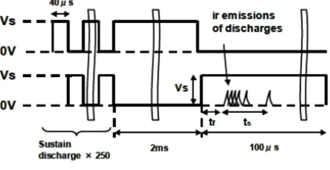
Then, we evaluate the discharge delay time. Figure 2 shows applied waveform cycle for discharge delay time measurements, where the discharge delay time consists of formation lag (tf) and statistical time-lag (ts). Firstly, 250 pulse are applied to a pair of surface discharge electrodes. After 2 ms as a period of nondischarge time, sustain pulse is applied to electrodes again for measuring the discharge delay. Discharge characteristics of MgO-PDP manufactured by using
“all-in-vacuum” process
T. Yano1,2, G. Uchida2, K. Uchida1, N. Awaji2, T. Shinoda2 and H. Kajiyama2
1Tsukuba Institute for Super Materials, ULVAC, Inc., Ibaraki, Japan
Tel.:81-29-847-8781, E-mail:[email protected]
2Graduate School of Advanced Sciences of Matter, Hiroshima University,
Higashi-Hiroshima, Japan
2-3 / T. Yano
IMID 2009 DIGEST •
The discharge delay time between the applied measurement pulse and the discharge emission is measured more than 1000 times.
Conventional process
Exhaust in the panel through glass tube MgO layer Alignment Sealing Gas filling ・Address electrode ・Dielectric layer ・Barrier ribs ・Phosphor layer ・Sealing layer ・ITO electrode ・Bus electrode ・Dielectric layer
Front panel Rear panel
In atmosphere
Conventional processExhaust in the panel through glass tube MgO layer Alignment Sealing Gas filling ・Address electrode ・Dielectric layer ・Barrier ribs ・Phosphor layer ・Sealing layer ・ITO electrode ・Bus electrode ・Dielectric layer
Front panel Rear panel
In atmosphere
“all-in-vacuum” process
Gas filling MgO layer Alignment Sealing Pre-baking ・Address electrode ・Dielectric layer ・Barrier ribs ・Phosphor layer ・Sealing layer ・ITO electrode ・Bus electrode ・Dielectric layerFront panel Rear panel
In vacuum
“all-in-vacuum” process
Gas filling MgO layer Alignment Sealing Pre-baking ・Address electrode ・Dielectric layer ・Barrier ribs ・Phosphor layer ・Sealing layer ・ITO electrode ・Bus electrode ・Dielectric layerFront panel Rear panel
In vacuum
Fig. 1 The flowchart of conventional and “al l-in-vacuum” process.
Fig. 2 Applied waveform cycle for tf and ts measurements.
3. Results and discussion
Figure 3 shows the aging characteristics of a conventional panel and the “all-in-vacuum” panel on aging time. The “all-in-vacuum” panel was stabilized in about 5 minutes, whereas the conventional panel was stabilized in about 120 minutes. This result indicates that the MgO surface has been kept clean in our process. This clearly demonstrates that our all-in-vacuum process is considerably effective for shortening the aging process leading to the cost reduction.
Figure 4 shows the discharge voltage of the conventional and the “all-in-vacuum” panels after aging process. The discharge voltage of “all-in-vacuum” panel was about 20V lower than that of the conventional one. This is almost consistent with the result of the panel manufactured by vacuum sealing process [2,3].
It should be noted that the difference in Vf1 and Vfn was 10V for “all-in-vacuum” panel and 25V for conventional panel. This result indicates that in a conventional process, the characteristics of MgO surface were inhomogeneous since the panel was exhausted through a glass tube before gas filling.
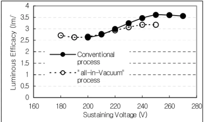
Figures 5 and 6 show the luminance and the luminous efficacy of the conventional and “all-in-vacuum” panels, respectively. No significant differences were measured. In ref. 2, the luminance and luminous efficacy of vacuum sealing panel were reported to be lower that those of conventional panel. The reason is not clear at this moment.
Figure 7 shows the discharge time-lag (tf + ts) of the conventional and “all-in-vacuum” panels as function of applied voltage. It is noteworthy that the discharge time-lag of “all-in-vacuum” panel was shortened by 60 % compared with a conventional panel. This result is almost consistent with the result
2-3 / T. Yano
• IMID 2009 DIGEST
of the panel manufactured by vacuum sealing process [2,3]. 140 180 220 260 300 340 380 420 0 30 60 90 120 150 180
aging time (min) D is ch ar ge V ol ta ge ( Vfn Vsmn Vfn Vsmn Conventional Process all-in-vacuum Process
Fig. 3 The dependence of discharge voltage of the conventional and vacuum process panel on aging time. 160 180 200 220 240 260 280 300
Conventional process "all-in-Vacuum" process D is ch ar ge V ol ta ge ( Vf1 Vfn Vsmn Vsm1
Fig. 4 Discharge voltage of the conventional and the vacuum process panel.
0 200 400 600 800 1000 1200 160 180 200 220 240 260 280 Sustaining Voltage (V) Lu m in an ce ( cd /m Conventional process "all-in-Vacuum" process
Fig. 5 Sustaining voltage dependence of luminance of the conventional and vacuum process panel. 0 0.5 1 1.5 2 2.5 3 3.5 4 160 180 200 220 240 260 280 Sustaining Voltage (V) Lu m in ou s Ef fic ac y (lm /W Conventional process "all-in-Vacuum" process
Fig. 6 Sustaining voltage dependence of luminous efficacy of the conventional and vacuum process panel. 0 0.5 1 1.5 2 2.5 3 3.5 160 180 200 220 240 260 280 Sustaining Voltage (V) tf + ts ( μs ) Conventional process "all-in-Vacuum" process
Fig. 7 Sustaining voltage dependence of discharge time lag of the conventional and vacuum process panel.
4. Summary
We have measured the discharge properties of the panels manufactured by using the “all-in-vacuum” process we have established [1]. It was confirmed that the “all-in-vacuum” process improves the aging time, discharge voltage and the discharge time-lag. This is the advantage of the “all-in-vacuum” process.
5. References
1. K. Uchida, G. Uchida, T. Yano, H. Kajiyama, and T.Shinoda, IDW08, PDP5-3.
2. C.-S. Park, H.-S. Tae,Y.-K. Kwon, S. B. Seo, E. G. Heo, and B.-H. Lee, SID Technical Digest, pp1434-1437(2007)
3. C.-S. Park, H.-S. Tae,Y.-K. Kwon, E. G. Heo, Mol