High aspect ratio silver grid transparent electrodes using UV embossing process
Dong Jin Kim, Mikyung Lim, Seung S. Lee, and Jin-Ha Kim
Citation: AIP Advances 7, 105218 (2017); View online: https://doi.org/10.1063/1.5009395
View Table of Contents: http://aip.scitation.org/toc/adv/7/10
Published by the American Institute of Physics
Articles you may be interested in
Metal grid/conducting polymer hybrid transparent electrode for inverted polymer solar cells
Applied Physics Letters 96, 203301 (2010); 10.1063/1.3394679
Mesh parameters influence on transparent and active antennas performance at microwaves
AIP Advances 7, 085120 (2017); 10.1063/1.4985746
Photovoltage responses of graphene-Au heterojunctions
AIP Advances 7, 105001 (2017); 10.1063/1.5001771
Competition between the inter-valley scattering and the intra-valley scattering on magnetoconductivity induced by screened Coulomb disorder in Weyl semimetals
AIP Advances 7, 105003 (2017); 10.1063/1.4998395
Accelerating large-scale phase-field simulations with GPU
AIP Advances 7, 105216 (2017); 10.1063/1.5003709
Thermochromic VO2 thin films on ITO-coated glass substrates for broadband high absorption at infra-red frequencies
High aspect ratio silver grid transparent electrodes
using UV embossing process
Dong Jin Kim,1Mikyung Lim,1Seung S. Lee,1and Jin-Ha Kim2,a
1Department of Mechanical Engineering, Korea Advanced Institute of Science and Technology,
Daejeon KS015, Korea
2Defense Agency for Technology and Quality, KS011 Jinju, Korea
(Received 10 May 2017; accepted 16 October 2017; published online 24 October 2017)
This study presents a UV embossing process to fabricate high aspect ratio silver grid transparent electrodes on a polymer film. Transparent electrodes with a high optical transmittance (93 %) and low sheet resistance (4.6 Ω/sq) were fabricated without any high temperature or vacuum processes. The strong adhesion force between the UV resin and the silver ink enables the fabrication of silver microstructures with an aspect ratio higher than 3. The high aspect ratio results in a low sheet resistance while maintaining a high optical transmittance. Multi-layer transparent electrodes were fab-ricated by repeating the proposed UV process. Additionally, a large-area of 8-inch touch panel was fabricated with the proposed UV process. The proposed UV process is a relatively simple and low cost process making it suitable for large-area produc-tion as well as mass producproduc-tion. © 2017 Author(s). All article content, except where otherwise noted, is licensed under a Creative Commons Attribution (CC BY) license (http://creativecommons.org/licenses/by/4.0/).https://doi.org/10.1063/1.5009395
Transparent electrodes are key elements in optoelectronic devices such as touch panels, organic solar cells, smart windows, transparent heaters, etc.1–4 They require high optical transmittance and low sheet resistance, which are determined by the materials, fabrication process, and pattern design used. Recently, in touch panel markets, flexible and large-area touch panels have gained much interest due to their application in wearable smart devices, touch monitors, electronic bulletin boards, etc. The development of transparent electrodes has moved towards including good flexibility and low sheet resistance in addition to high transmittance.5
Indium tin oxide (ITO) has been the most widely used material for transparent electrodes for decades. The disadvantages of ITO is its limited sheet resistance at high transmittance and poor flex-ibility.6These disadvantages are not suitable for large-area touch screen panels or flexible devices.
Much research has been done on alternative materials such as conductive polymers,7,8 carbon
nan-otubes,9,10graphene films,11,12metal nanowires,13,14and metal grids.15–17Among them, metal grids
are considered as a promising alternative transparent electrode with high optical transmittance, low sheet resistance, and good flexibility.
A metal grid is comprised of microscale patterns consisting of a metal such as gold, silver, or copper. A high aspect ratio of metal grids is an essential requirement to achieve a low sheet resistance at high transmittance because metal grids have a trade-off between the optical transmittance and the sheet resistance. Recently, many studies have investigated the fabrication of metal grids with printing processes such as offset, ink jet, and gravure printing processes, which have an aspect ratio lower than 1.18–20
This paper introduces a UV embossing process to fabricate metal grid transparent electrodes with a high aspect ratio (∼3). The silver ink has a high conductivity and low annealing temperature. The UV resin functions as an adhesion layer between the silver ink and a polymer film, which has a strong enough adhesion force to transfer the silver ink to the polymer film. The heat generated by the UV lamp hardens the silver ink, which results in a high aspect ratio without any disruptions. Multi-layer transparent electrodes were obtained on a single polymer film by repeating the proposed
aAuthors to whom correspondence should be addressed. Electronic mail:kimjinha20@dtaq.re.kr
105218-2 Kim et al. AIP Advances 7, 105218 (2017) UV process because the UV resin functions as both an electrical insulation layer and an adhesion layer. The proposed UV process is a relatively simple and low cost process, which is suitable for mass production.
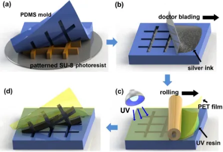
Figure1illustrates the UV embossing process for fabricating high aspect ratio silver grid trans-parent electrodes. SU-8 photoresist structures are patterned on a silicon substrate with various line widths (3.5 ∼ 10 µm), heights (8 ∼ 21 µm), and pitches (200 ∼ 800 µm). To replicate the SU-8 photoresist structures, polydimethylsiloxane (PDMS) is poured onto the patterned SU-8 photoresist structures and then cured at 65oC for 90 min. in a convection oven (Figure 1(a)). The silver ink (Fine Paste, Korea, FTL-201NF), which has silver particle size of 500 nm and viscosity 15000 cps, is dispensed onto the PDMS mold and filled into the replicated patterns by the doctor blading process under constant pressure (5 MPa) and speed (50 mm/s) (Figure1(b)). It is important to optimize the pressure of the doctor blading process because at high pressure, the silver ink does not sufficiently fill the replicated patterns, while at low pressure, silver ink residue remains decreasing the transmittance. The optimized pressure is obtained by gradually increasing from low pressure until silver ink residue does not remain. The UV resin (CC Tech, Korea, NE-0425) is dispensed onto the PDMS mold, and then, the polyethylene terephthalate (PET) film (SKC, Korea, SH40) is attached with a roller. After the UV exposure process by mercury UV lamp (100mW/cm2) for 30 sec., the UV resin is cured, and the silver ink is somewhat hardened due to heat of the UV curing chamber (Figure1(c)). By peeling off the PET film, the silver ink grid structures are transferred to the PET film (Figure1(d)). Finally, the silver ink grid on the PET film is annealed at 100oC for 30 min. in a convection oven.
The strong adhesion force of the UV resin enables the fabrication of a high aspect ratio silver ink grid; moreover, it overcomes the friction force between the silver ink and the PDMS mold. The proposed UV process is relatively simple and does not require expensive facilities.
Figure2 shows the SEM images of a silver ink grid and some arbitrary shapes. A silver ink grid with a 5 µm line width and 15 µm pitch is shown in Figure2(a), which is uniformly fabricated without any defects despite the high density grid structures. Figure2(b)and(c)show SEM images of the silver ink lines with an aspect ratio higher than 3 which enables a low sheet resistance while maintaining a high optical transmittance. Figure2(d)shows arbitrary shaped silver ink. It was easy to fabricate the arbitrary shaped silver ink and silver ink line with various line widths at the same time.
Figure3(a)shows a touch panel for a smart phone. The silver ink lines, which have a different line width and pitch, are clearly connected. According to the design of the grid structures, touch sensing
FIG. 1. Schematic illustration of the UV embossing process flow (a) replicating the PDMS mold with patterned SU-8 pho-toresist structures, (b) dispensing and doctor blading the silver ink, (c) coating and curing the UV resin between the PDMS mold and the PET film, (d) peeling off the PET film from the PDMS mold.
FIG. 2. SEM images of a silver ink grid and arbitrary shapes. (a) a silver ink grid with a 5 µm line width and 15 µm pitch, (b) and (c) silver ink lines with a line width of 3.5 µm and an aspect ratio of ∼ 3, (d) arbitrary shaped silver ink.
FIG. 3. (a) A touch panel for a smart phone, (b) array of LED chips on the silver ink grid transparent electrodes.
electrodes (inside the blue line) and connection electrodes (inside the red line) are fabricated by only a single process at the same time. Figure3(b)shows an array of light emitting diode (LED) chips on the silver ink grid transparent electrodes. LED chips are connected to each transparent electrode which are separated by 10 µm. Even though the separation gap of the adjacent electrodes is very small, the LED chips operate without any shorts because the UV resin functions as an insulator between the electrodes.
After cutting the silver ink line structures with a focused ion beam (FIB), the interfaces between the silver ink and UV resin could be observed as shown in Figure4(a)–(c). The shrinkage of the silver ink forms a parabolic shape at the interface during the UV exposure process, which depends on the amount of silver ink. The height of the UV resin was also different depending on the height of the silver ink. As the height of the silver ink increases, the height of the UV resin also increases. In order
FIG. 4. Cross section images of silver ink line structures. (a)-(c) silver ink lines with heights of 7 µm, 11 µm, and 15 µm starting from the left side, respectively.
105218-4 Kim et al. AIP Advances 7, 105218 (2017) to increase the height of the silver ink, the trench of the mold should be deep. The deeper the trench of the mold, the greater the amount of silver ink filled in the mold. The larger the amount of silver ink, the larger the amount of evaporated solvent, thereby the larger the shrinkage. Therefore, since the void space of the mold is relatively large, the UV resin is filled more inside the mold. As a result, the height of the UV resin increases. The strong bond between the silver ink and the UV resin at the interface enables the fabrication of a high aspect ratio silver ink gird.
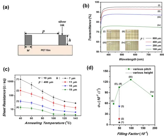
Transmittance and sheet resistance are the most important performance factors of transparent electrodes. The design of the silver grid pattern enables adjustments to its performance. Figure5(a) shows the design factors of the silver ink grid transparent electrodes which are expressed as the line width (w), pitch (p), and height (h). The filling factor ( fF) directly reflects the characteristics of the
transmittance and sheet resistance, and it is defined as follows: fF= 1 −
( p − w)2
p2 (1)
Figure5(b)shows the relationship between the transmittance@ 550 nm, w/o substrateand the filling factor of the silver ink grid transparent electrodes with a w and h of 10 and 19 µm, respectively. The values for fF, which are (i) 0.025, (ii) 0.049, (iii) 0.098, and (iv) 0.190, were calculated with equation (1)
for different p of 800, 400, 200 and 100 µm, respectively. The highest transmittance of 95 % corre-sponded to an fF of 0.025. The others were 93, 88, and 76 % when the fF were 0.049, 0.098, and
0.190, respectively. From the fF, it is possible to calculate the transmittance (T ) with the following
equation:
T= 1 − fF (2)
The calculated values using equation (2) were 98, 95, 90, and 81 % which are slightly higher than the measured values because the transmittance decreases due to UV resin layer and any remaining silver ink residues.
FIG. 5. (a) Design factors of the silver ink grid transparent electrodes, (b) transmittance vs. filling factor, (c) sheet resistance vs. annealing temperature and height of the silver ink, (d) ΦTEvs. height of filling factor.
In Figure5(c), the sheet resistances were measured according to the annealing temperature and height of the silver ink with a w and p of 10 and 400 µm, respectively. The sheet resistances with lower value are obtained at the higher annealing temperature. However, since PET film is deformed at 140oC or more, the annealing temperature for lowest sheet resistance is 100oC. After annealing at 100 oC for 30 min., the sheet resistances with the h of 7, 11, 15, and 19 µm were 74.1, 29.1, 9.3, and 4.6 Ω/sq, respectively. The sheet resistance decreases by increasing the height of the silver ink without any loss of transmittance because the thickness of the silver grid is not related to the transmittance.
The transparent electrodes have a trade-off relation between the transmittance and the sheet resistance. To optimize the performance factors, a figure-of-merit (ΦTE) is introduced by Haacke.21 The ΦTEis defined by Haacke’s equation as follows:
ΦTE=
T10 Rs
(3) where Rsis the sheet resistance. Figure5(d)shows the figure-of-merit calculated by Equation (3). The
transparent electrode with a T of 88% and a Rsof 2.2 Ω/sq had the highest ΦTEvalue of 0.126 when the fFand h was 0.098 and 19 µm. For a transmittance higher than 90%, the transparent electrode with a T of 93% and a Rsof 4.6 Ω/sq had a ΦTEvalue of 0.105 when the fFand h was 0.049 and 19 µm. Among the electrodes of various heights with a fF of 0.049, the transparent electrode with
a h of 19 µm had the highest ΦTE. Thus, the high aspect ratio structure of the silver ink has a high figure-of-merit because high aspect ratio silver grid reduce the sheet resistance without decrease of transmittance.
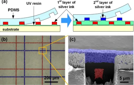
Figure6(a)shows the fabrication process for the multi-layer silver ink transparent electrode. A double-layer silver ink transparent electrode was fabricated by repeating the proposed UV process using the already fabricated transparent electrode as a substrate. Figure6(b)shows the microscope image of the top view of the double-layer silver ink transparent electrode. The red and blue lines represent the first and second layer of the silver ink, respectively. The cross section view shows that the UV resin acts as an electrical insulator between the silver ink electrodes of both layers. The electrical insulation characteristics of the UV resin is well suited for the touch panel with the double-layer transparent electrode (Figure6(c)).
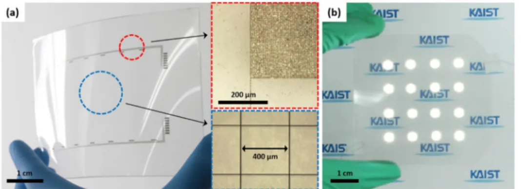
Figure7(a)shows the fabrication result of a large-area (16 × 19 cm2) silver ink grid transpar-ent electrode, which shows that the proposed UV process is suitable for application to large-area transparent electrodes such as a touch panel or tablet computer. It was relatively easy to fabricate the large-area transparent electrode because the silver ink grid was directly transferred to a PET film.
FIG. 6. (a) Fabrication process of the multi-layer silver ink transparent electrode. (b) and (c) microscope image of the top view and SEM image of the cross section view of the multi-layer silver ink structures.
105218-6 Kim et al. AIP Advances 7, 105218 (2017)
FIG. 7. (a) Fabrication result of a large-area (16 × 19 cm2) silver ink grid transparent electrode, (b) and (c) images of an 8-inch touch panel and demonstration of touch sensing (seesupplementary material).
The resistive touch panel needs to two transparent electrodes and spacer separating the both electrodes. The pressure by the touch causes that the upper electrode contacts the lower electrode, and then the position of the touch can be detected by sensing the electrical signal. The large-area silver ink grid transparent electrode was applied to an 8-inch touch panel by laminating the lower ITO electrode. The touch sensing was demonstrated by writing “KAIST” with a finger shown in Figure7(b)and(c). Given that touch sensing electrodes and connection electrodes are fabricated at the same time, the proposed UV process can improve the production rate for mass production.
In this paper, we present a UV embossing process to fabricate high aspect ratio (∼3) silver ink grid transparent electrodes with a line width of 3.5 µm. The high aspect ratio structure increases the conductivity while maintaining the transmittance of the metal grid type transparent electrode. Various printing processes are difficult to achieve with an aspect ratio of 1 or more. The high aspect ratio of the transparent electrodes decreases the sheet resistance while maintaining high transmittance. The silver ink grid transparent electrodes have a transmittance of 93 % and a sheet resistance of 4.6 Ω/sq. This result has better performance than silver grid transparent electrodes fabricated with printing processes or other fabrication processes such as electrohydrodynamic jet printing22and laser sintering.23The UV embossing process can fabricate low sheet resistance and large-area (16 × 19 cm2) transparent electrodes. Touch sensing electrodes and connection electrodes can be fabricated at the same time because the proposed UV process replicates the patterns of a PDMS mold. Moreover, multi-layer transparent electrodes can be fabricated by an iterative process on a single substrate. Our process, which is relatively simple, is suitable for mass production and does not require high temperature, vacuum processes, and expensive facilities. Furthermore, we believe that high aspect ratio structure has advantage in gas sensors and bio-chemical applications.
SUPPLEMENTARY MATERIAL
Seesupplementary materialfor demonstration of touch sensing.
ACKNOWLEDGMENTS
This work was supported by the National Research Foundation of Korea(NRF) grant funded by the Korea government(MEST) (No. 2017-011192) and Brain Korea 21(BK 21) Plus Program.
1H.-G. Im, B. W. An, J. Jin, J. Jang, Y.-G. Park, J.-U. Park, and B.-S. Bae,Nanoscale8, 3916 (2016).
2K. A. Bush, C. D. Bailie, Y. Chen, A. R. Bowring, W. Wang, W. Ma, T. Leijetens, F. Moghadam, and M. D. Mcgehee,Adv.
Mater.28, 3937 (2016).
3H. H. Khaligh, K. Liew, Y. Han, N. M. Abukhdeir, and I. A. Goldthorpe,Sol. Energ. Mat. Sol. C.132, 337 (2015). 4Q. Huang, W. Shen, X. Fang, G. Chen, J. Guo, W. Xu, R. Tan, and W. Song,RSC Adv.5, 45836 (2015). 5Seehttp://technology.ihs.com/530896for “Touch panel market update” (last accessed May 8, 2015). 6K. A. Sierros, N. J. Morris, K. Ramji, and D. R. Cairns,Thin Solid Films517, 2590 (2009).
7Y. Wang, C. Zhu, R. Pfattner, H. Yan, L. Jin, S. Chen, F. Molina-Lopez, F. Lissel, J. Liu, N. I. Rabiah, Z. Chen, J. W. Chung,
C. Linder, M. F. Toney, B. Murmann, and Z. Bao,Sci. Adv.3, e1602076 (2017).
8X. Zhang, J. Wu, J. Wang, J. Zhang, Q. Yang, Y. Fu, and Z. Xie,Sol. Energ. Mat. Sol. C.144, 143 (2016). 9L. P. Yu, C. Shearer, and J. Shapter,Chem. Rev.116, 13413 (2016).
10S. N. Habisreutinger, R. J. Nicholas, and H. J. Snaith,Adv. Energy Mater.7, 1601839 (2017). 11Y. Xu and J. Liu,Small12, 1400 (2016).
12H. Jang, Y. J. Park, X. Chen, T. Das, M.-S. Kim, and J.-H. Ahn,Adv. Mater.28, 4184 (2016). 13C.-H. Song, C. J. Han, B.-K. Ju, and J.-W. Kim,ACS Appl. Mater.8, 480 (2016).
14W. Xiong, H. Liu, Y. Chen, M. Zheng, Y. Zhao, X. Kong, Y. Wang, X. Zhang, X. Kong, P. Wang, and L. Jiang,Adv. Mater.
28, 7167 (2016).
15S. Jang, W.-B. Jung, C. Kim, P. Won, S.-G. Lee, K. M. Cho, M. L. Jin, C. J. An, H.-J. Jeon, S. H. Ko, T.-S. Kim, and
H.-T. Jung,Nanoscale8, 14257 (2016).
16W. Zhou, J. Chen, Y. Li, D. Wang, J. Chen, X. Feng, Z. Huang, R. Liu, X. Lin, H. Zhang, B. Mi, and Y. Ma,ACS Appl.
Mater.8, 11122 (2016).
17Y. Liu, S. Shen, J. Hu, and L. Chen, Opt. Express 24, 25574 (2016).
18I. Kim, S.-W. Kwak, Y. Ju, G.-Y. Park, T.-M. Lee, Y. Jang, Y.-M. Choi, and D. Kang,Thin Solid Films580, 21 (2015). 19P.-C. Yu, C.-C. Hong, and T.-M. Liou,J. Micromech. Microeng.26, 035012 (2016).
20J. Park, H. A. D. Nguyen, S. Park, J. Lee, B. Kim, and D. Lee,Curr. Appl. Phys.15, 367 (2015). 21G. Haacke,J. Appl. Phys.47, 4086 (1976).
22Y. Jang, J. Kim, and D. Byun,J. Phys. D: Appl. Phys.46, 155103 (2013).