50-1 / B.-S.Jeong
• IMID 2009 DIGEST
Abstract
a-IGZO is an attractive material to make an AMOLED device with uniform TFT properties for use in a large size display. However, this material shows TFT properties that are very sensitive to water or hydrogen. Therefore, it is essential to control these critical factors during fabrication of the backplane in order to improve the TFT performance. In this paper, we report the effect of passivation layer properties on the performance of the oxide TFTs.
1. Introduction
Recently, a-IGZO semiconductor materials have attracted considerable attention for their potential application to transparent electronics. One of the possible applications is their use as a TFT backplane for large size AMOLED TV. a-Si TFTs show uniform TFT properties in large size displays, but they are unstable for use in current driving mode. However, a-IGZO, which has an ionic bond, has been shown to be very stable for OLED driving current [1]. This significant advantage makes a-IGZO TFT one of the leading candidates to enable large size AMOLED devices. It also shows much higher electron mobility compared to a-Si TFT in an inverted staggered type structure as shown in fig. 1. However, this material shows TFT properties that are very sensitive to water or post processing parameters such as deposition temperature [2]. In order to improve the TFT quality, it is necessary to precisely control post fabrication processes. However, few papers have addressed these post processing parameters.
In this paper, we report the effect of passivation layer properties on the performance of oxide TFTs.
2. Experiments
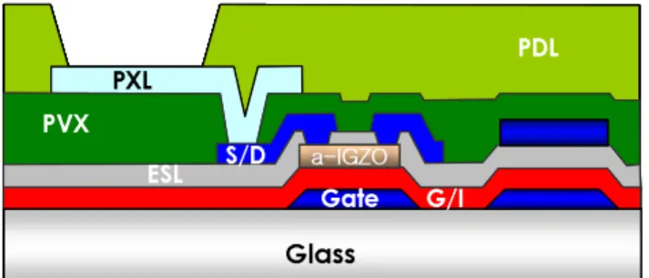
Fig. 1 shows the schematic diagram of an a-IGZO TFT structure. An inverted staggered etch stopper structure was used for the fabrication of oxide TFTs. Molybdenum tungsten (MoW) metal was patterned by wet etching to form the gate. Tetraethyl orthosilicate (TEOS) materials were deposited to form the gate insulator. A 50nm thick layer of a-IGZO film (Ga2O3: In2O3: ZnO = 2:2:1 atomic %) as an active layer were deposited by DC magnetron sputtering at 100°C.
TFT G/I ESL S/D PVX PXL PDL Glass Gate G/I ESL S/D PVX PXL PDL a-IGZO TFT G/I ESL S/D PVX PXL PDL Glass Gate G/I ESL S/D PVX PXL PDL a-IGZO
Fig. 1 Schematic diagram of a-IGZO TFT
Effect of Passivation Layer Properties on the
Performance of Oxide TFTs
Byoung-Seong Jeong, Chang-Mo Park, Mu-Gyeom Kim, Hyun-Joong
Chung, Tae-Kyung Ahn, Seong-Kweon Heo, Jong-Han Jeong, Min-Kyu
Kim, Hye-Hyang Park, Jong-Moo Huh, Yeon-Gon Mo, Hye-Dong Kim,
Sang Soo Kim
OLED R&D Center, Samsung Mobile Display Co., LTD.,
Giheung-Gu, Yongin-City, Gyeonggi-Do, Korea
Tel.:+82-31-209-9689, E-mail: [email protected]
50-1 / B.-S.Jeong
IMID 2009 DIGEST • In order to prevent active a-IGZO over-etch, an etch
stopper layer was deposited on the active a-IGZO and contact is made with S/D through a via hole. There is no wet etch selectivity for active a-IGZO during S/D (MoW/AlNd/MoW) wet etch. The bottom layer of the MoW S/D metal and the active a-IGZO have good ohmic contact. There was no current crowding at low Vds on the output curve of the a-IGZO TFTs. The TFT was annealed at 350°C to control conductivity of the a-IGZO film.
Carrier concentration and resistivity of a-IGZO was measured by Hall measurement (Nano-Metrics HL 5500). The thickness of deposited films was evaluated using an ellipsometer. TFT properties were measured by an HP 4156 system.
3. Results and discussion
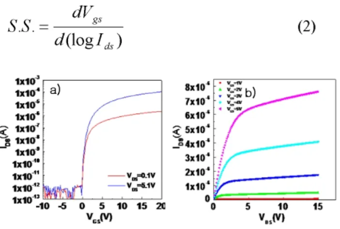
Fig. 2 shows single TFT properties of a-IGZO films. A single etch stopper layer was deposited. Threshold voltage (Vth), which was defined at Ids equal to 10nA times W/L, was 0.95V and saturation mobility was 23.5cm2/V-sec. Saturation mobility was measured at Vds= 5.1V. Saturation mobility (µFE) was extracted from the saturation current equation of a field-effect transistor. 2 ) ( 2L Vgs Vth W C I FE ox ds = µ − (1) Where Cox is gate insulator capacitance per unit area, W and L are channel width and length, respectively. Sub-threshold swing (S.S.) was 0.27V/dec. S.S. can be extracted over the range of 10-10A and 10-8A of I
ds using the following equation:
) (log . . ds gs I d dV S S = (2)
Fig. 2 Single TFT properties of a-IGZO films (a) I-V curve (b) output curve (W/L=25/8µm)
Fig. 3 shows TFT property dependence on the different etch stopper layer (ESL) material. Fig. 3(a) shows TFT properties measured at Vds=10.1V for a SiOx etch stopper layer deposited at 300°C by a PECVD system. Fig. 3(b) shows TFT properties which were measured 4 times at Vds=10.1V for a TEOS ESL layer grown at 400°C by the same system. In order to prevent a TFT short as in fig. 3(a), a double layer ESL was applied for both materials. The bottom layer was grown by SiOx 150nm at 150°C and the top was deposited by those layers mentioned above. As shown in Fig. 3, SiH4 based SiOx ESL layer shows a TFT short, but TEOS layer shows excellent TFT properties even though this material was deposited at a much higher temperature, around 400°C. The reaction equations for the growth of each layer follow:
SiH4 + 2N2O SiO2 + 2N2 + 2H2 (for SiOx) (3) Si(OC2H5)4 + O2 + He SiO2 + 4O(C2H5)
(for TEOS) (4)
For SiH4 based SiOx, much more hydrogen is generated after the reaction compared to TEOS. This hydrogen may exhibit a very rapid diffusion in a-IGZO when incorporated by plasma exposure. Diffusivity of hydrogen in ZnO by plasma exposure has been measured as D of 8.7x1010cm2/V-s at 300°C [3]. However, all of the plasma-incorporated hydrogen is removed from the ZnO by annealing at 500°C. The free electron concentration increases after plasma hydrogenation, consistent with the small ionization energy predicted for H in ZnO.
Fig. 3 Comparison of TFT properties depending on the different etch stopper layer. (a) SiOx (b) TEOS (W/L=50/8.5µm)
In case of a-IGZO, carrier concentration can be increased by free hydrogen incorporation, with the result that the device no longer works as a field effect transistor. For many other semiconductor materials it has been shown that hydrogen introduced, e.g. from a
50-1 / B.-S.Jeong
• IMID 2009 DIGEST
plasma at relatively low temperatures, readily forms complexes with various donor and acceptor species and often renders them electrically neutral (the phenomenon widely known as hydrogen passivation). There seems to be general agreement that hydrogen can be introduced relatively easily from hydrogen plasma at moderate temperatures such as 200–300°C.
Fig. 4 shows SIMS profiles of a ZnO sample exposed to 2H plasma of 0.5h at 200°C, then annealed for 5 min under N2 at different temperatures [3]. There is significant loss of 2H even after a short anneal at 400°C, with virtually all of it evolved out of the crystal by 500°C. This is in sharp contrast to 2H in GaN, where much higher temperatures (>800 °C) are needed to evolve the deuterium out of the sample [4, 5].
Fig. 4 SIMS profiles of 2H in ZnO after annealing
over 400°C for 5 min.
The 2H plasma treatment causes an increase in donor concentration. In that case, the effect was attributed to hydrogen passivation of compensating acceptor impurities present in the as-grown ZnO epitaxial layers. An alternative explanation is that the hydrogen induces a donor state and thereby increases the free electron concentration [3].
Fig. 5 shows TOF-SIMS results for the cross-section of the SiOx(PVX/ESL)/a-IGZO/TEOS(G.I.). As shown in fig. 5, the hydrogen peak exists around the interface of the ESL and the a-IGZO active layer. However, an OH- peak exists through the whole area of a-IGZO and shows a decreasing trend from the top of a-IGZO to the interface of a-IGZO and TEOS gate insulator. The hydrogen may easily exist as OH- in the a-IGZO and those hydrogen dopants probably act as donors. This effect results in increasing conductivity of the a-IGZO film with a resultant negative Vth shift in the TFT. Further investigation on these phenomena is still underway.
SiOx (PVX/ESL) a-IGZOTEOS SiOx (PVX/ESL) a-IGZOTEOS
Fig. 5 TOF-SIMS results for the cross-section of the SiOx(PVX/ESL)/a-IGZO/TEOS(G.I.)
It has not yet been confirmed that the increase of carrier concentration came only from the hydrogen incorporation. It likely arises from multiple sources such as hydrogen plasma exposure and post-deposition temperature.
We must at least take into account the electrical activity and rapid diffusivity of H in a-IGZO when designing device fabrication processes such as deposition of dielectrics using SiH4 as a precursor, or dry etching involving use of CH4/H2/Ar plasmas, since these could lead to significant changes in near-surface conductivity.
4. Summary
In summary, we have investigated effects of the passivation layer properties on performance of oxide TFTs. TFT properties were obtained from a TEOS-based SiOx etch stopper layer, but not from SiH4 -based SiOx. This difference in TFT performance is likely caused by hydrogen incorporation during the growth of the etch stopper layer after the active a-IGZO process. In order to improve the performance of a-IGZO TFTs, we conclude that it is critical to control hydrogen incorporation during device fabrication.
5. Acknowledgements
The authors wish to thank all project members working on the development of oxide TFTs at Samsung Mobile Display. We also are grateful for the helpful support of the Samsung Advanced Institute of Technology.
50-1 / B.-S.Jeong
IMID 2009 DIGEST •
6. References
[1] K. Nomura, H. Ohta, A. Takagi, T. Kamiya, M. Hirano, and H. Hosono, Nature 432, 488 (2004). [2] J.K. Jeong, H.W. Yang, J.H. Jeong, Y.G. Mo, H.D. Kim, Appl. Phys. Letters 93, 123508 (2008).
[3] S.J. Pearton, D.P. Norton, K. Ip, Y.W. Heo, T. Steiner, Progress in Materials Science 50, p.293 (2005).
[4] Pearton S. J., Zolper J. C., Shul R. J., Ren F., J Appl Phys 86, pp1 (1999).
[5] Auret FD, Goodman SA, Hayes M, Legodi MJ, Van Laarhoven HA, Look DC. Appl Phys Lett 79, p. 3074 (2001).
![Fig. 4 shows SIMS profiles of a ZnO sample exposed to 2 H plasma of 0.5h at 200°C, then annealed for 5 min under N 2 at different temperatures [3]](https://thumb-ap.123doks.com/thumbv2/123dokinfo/4876416.33916/3.892.468.824.148.352/sims-profiles-sample-exposed-plasma-annealed-different-temperatures.webp)
