32-3 / S. Yang
IMID 2009 DIGEST •
Abstract
We fabricated oxide and oxide/organic hybrid TFTs on a glass substrate using the photolithography process under 200ºC. We adopt the solution processed organic ferroelectric materials of P(VDF-TrFE) and polyimide (KSPI) insulator for 1-T structure memory and flexible device, respectively. All devices have successfully operated and showed the possibility of hybrid TFTs for the application to the flexible electronic devices.
1. Introduction
Flexible displays have attracted many attentions because of their rugged, lightweight, and conformable or rollable properties. [1] Despite the merits of flexible devices, many restrictions existed in the fabrication of flexible display, which contain the substrate handling problem, barrier properties of plastic substrate, no suitable back-plane. Recently, oxide TFTs processed at a low-temperature showed good electrical properties such as mobility, uniformity, and sub-threshold swing so that it is promising to fabricate the flexible devices based on the oxide TFTs.
[2, 3] Since inorganic based insulator have the relatively poor insulation properties than organic insulators by the low-temperature process, the studies on the oxide/organic hybrid TFTs composed of the oxide semiconductors and organic insulator are needed. There are some reports on the hybrid TFTs fabricated by the shadow mask process. Photolithography process related to the chemical resistivity of organic materials and stability characteristics are not reported yet. [4] In this paper,
we showed high performance hybrid TFTs with high on/off ratio and mobility. Furthermore bias stability characteristics of hybrid TFTs will be mentioned in the conference.
2. Experimental
We fabricated the three-type TFTs with staggered structure based on an AT-ZIO (Al-Sn-Zn-In-O) oxide semiconductors, which have the Atomic Layer Deposition (ALD) grown Al2O3 inorganic insulator,
spin-coated KSPI and poly(vinylidene fluoride-trifluoroethylene) [P(VDF-TrFE)] insulators, respectively.
Figure 1. Cross-sectional view of fabricated devices All devices were patterned by using the conventional photolithography and wet/dry etching process. 150nm-thick ITO (In-Sn-O) source/drain electrode was deposited by rf sputter and patterned by wet-etching process. AT-ZIO active layer was deposited by rf magnetron sputter, which was formed by co-sputtering method using the AZO (Al-Zn-O) and ITO target. Then 9nm-thick Al2O3 protection layer (PL)
layer was grown by means of the ALD method using
Oxide/Organic Hybrid TFTs for Flexible Devices
1,3ShinHyuk Yang, 1Doo-Hee Cho, 1Sang-Hee Ko. Park,1Jeong-Ik Lee, 1Woo-Seok Cheong, 1Sung-Min Yoon, 1Min-Ki Ryu, 1Chunwon Byun, 1
Oh-Sang Kwon, 1Kyoung-Ik Cho,1Hye Yong Chu, *1Chi-Sun Hwang, 2Taek
Ahn, 2Yoojeong Choi, 2Mi Hye Yi, and 3Jin Jang
1Transparent Electronics Team, ETRI, 138 Gajeong-ro,Daejeon 305-350 Republic of
Korea
Tel.:82-42-860-1149, E-mail: [email protected]
2
Information and Electronics Polymer Research Center, KRICT, Daejeon 305-600,
Republic of Korea
3
Dept. of Information Display, Kyung-Hee University, Seoul, Republic of Korea
32-3 / S. Yang
• IMID 2009 DIGEST
the trimethyl aluminum (TMA) as an Al precursor and H2O as an oxygen precursor. Both active and PL layer
was simultaneously patterned by wet-etching process.
[5] 176nm-thick Al2O3 insulator (device A) was grown
using the same method with PL layer and patterned by wet-etching process. About 300nm-thick KSPI insulator (device B) and 100nm-thick P(VDF-TrFE) ferroelectric layer (device C) was spin-coated and patterned by dry-etching method using the oxygen plasma. Then devices were annealed at 160ºC and 140 ºC to remove the solvent and form the β-phase of organic ferroelectric materials. [6] KSPI organic insulators, provided by KRICT, have the several merits such as low-temperature process of 160 ºC and good insulation properties. [7] P(VDF-TrFE) organic ferroelectric layer is widely used materials for organic memory device and the pattern formation using the photolithography process is difficult largely due to the chemical inertness and adhesion problem. By using the 1-T (1 transistor) structure instead of 1T-1C (1 transistor 1capacitor) structure, high integration and low power consumption properties also can be obtained. 150nm-thick ITO gate electrode was deposited on the Al2O3 and KSPI insulators and
150nm-thick Al gate electrode was deposited on the P(VDF-TrFE) thin film. ITO and Al gate electrode pattern was formed by wet-etching process. Finally, both device A and B were annealed at 200 ºC and device C was annealed at 140 ºC. Limited anneal temperature of device C is mainly related to the ferroelectric phenomenon and device A and B is related to the optimization and removal of solvent and water residue in TFTs. Figure 1 and Table 1 shows the device structure and process summary of each device. All measurements were carried out in the dark box, using the Agilent semiconductor parameter analyzer B1500A, and double sweep modes are also used to see the hysteresis characteristics.
S/D Active GI Gate Anneal T (ºC) Device A Al2O3 ITO 200ºC Device B KSPI ITO 200ºC Device C
ITO AT-ZIO
P(VDF-TrFE) Al 140ºC Table 1. Summary of fabrication process and layer
3. Results and discussion
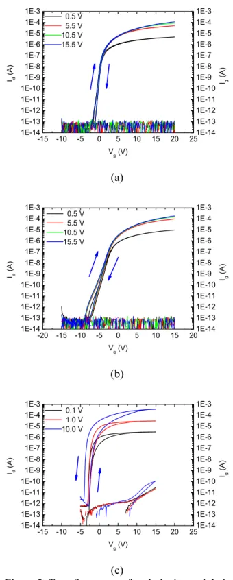
Table 2 shows the electrical parameters of each TFTs and Figure 2 (a)~(c) shows the measured transfer
curves of each devices in the air ambient.
(a)
(b)
(c)
Figure 2. Transfer curves of each device and their hysteresis direction, for AlOx insulator (a), KSPI
32-3 / S. Yang
IMID 2009 DIGEST •
µsat
(cm2/Vs) (V) VT V(V) on (V/decade) SS slope Ionratio -Ioff
Device A 9.15 0.59 -1.41 0.36 1.1E9
Device B 7.94 -1.90 -8.18 1.0 1.9E9
Device C 25.13 0.41 -4.25 0.13 3.6E8
Table 2. Electrical parameter of device A, B (VD=15.5
V), and C (VD=10.0 V)
Although there is some variation of the turn-on voltage (Von), all devices showed well behaved TFT
performance. In case of device C, we obtained the counterclockwise hysteresis characteristics implying the memory window. The variation of SS slope and mobility in each device are also observed. We believe that it is mainly concerned with the difference of capacitance value of each insulator, which is related to the insulator thickness and dielectric constant of each layer. (measured capacitance value of device A, B, and C is about 3.6E-8 F/cm2, 1.05E-8 F/cm2, 1.09E-7
F/cm2, respectively.)
Finally, we will show the bias stability characteristics of oxide/organic hybrid TFTs under the air and vacuum conditions at the conference hall.
4. Summary
We fabricated oxide and oxide/organic hybrid TFTs using the ALD grown Al2O3, low-temperature
processable polyimide (KSPI), and ferroelectric P(VDF-TrFE). All devices showed high on-off ratio (>108) and saturation mobility. Considering the
electrical characteristics of hybrid TFTs, it is promising to fabricate the flexible devices based on the organic insulator and oxide semiconductors.
Acknowledgement
This work was supported by the IT R&D program of MKE/KEIT [2006-S079-04, Smart window with transparent electronic devices]. This research was supported by the 21st century Frontier R&D Program funded by the Ministry of Knowledge Economy of Korean government.
5. References
[1] Chang-Dong Kim, In-Byeong Kang, and In-Jae
Chung, SID Technical Digest, pp. 1669-1672 (2007)
[2] Doo-Hee Cho, Shinhyuk Yang, Chunwon Byun,
Min Ki Ryu, Sang-Hee Ko Park, Chi-Sun Hwang, Sung Min Yoon, and Hye-Yong Chu, IEEE Electron Device Lett., Vol. 30, No. 1, January 2009
[3] Jin-Seong Park, Tae-Woong Kim, Denis
Stryakhilev, Jae-Sup Lee, Sung-Guk An, Yong-Shin Pyo, Bum Lee, Yeon Gon Mo, Dong-Un Jin, and Ho Kyoon Chung, Appl. Phys. Lett., 95, 013503 (2009)
[4] Kimoon Lee, Jae Hoon Kim, and Seongil Im,
Appl. Phys. Lett., 88, 023504 (2006)
[5] Sang-Hee K. Park, Chi-Sun Hwang, Minki Ryu,
Shinhyuk Yang, Chunwon Byun, Jaeheon Shin, Jeong-Ik Lee, Kimoon Lee, Min Suk Oh, and Seongil Im, Adv. Mat., Vol. 21, pp. 678-682, 2009
[6] R. C. G. Naber, C. Tanase, P. W. M. Blom, G. H.
Gelinck, A. W. Marsman, F. J. Touwslager, S. Setayesh, and D. M. De Leeuw, Nature Materials, Vol. 4, March 2005, pp. 243-248
[7] Taek Ahn, Jin Woo Kim, Yoojeong Choi, and Mi
Hye Yi, Organic Electronics Vol. 9, 2008, pp. 711-720