Silicon Photonic MEMS Phase-Shifter
H
AMEDS
ATTARI,
1,*T
EODOROG
RAZIOSI,
1M
ARCELLK
ISS,
1T
AEJ
OONS
EOK,
2S
ANGYOONH
AN,
3M
INGC. W
U,
4ANDN
IELSQ
UACK1 1École Polytechnique Fédérale de Lausanne (EPFL), Lausanne, Switzerland 2Gwangju Institute of Science and Technology, Gwangju 61005, Republic of Korea 3Korea Advanced Institute of Science and Technology, Daejeon 34141, Republic of Korea4Department of Electrical Engineering and Computer Sciences, University of California, Berkeley, CA, 94720, USA
*hamed.sattari@epfl.ch
Abstract: We present a design for an analog phase shifter based on Silicon Photonic MEMS technology. The operation principle is based on a two-step parallel plate electrostatic actuation mechanism to bring a vertically movable suspended tapered waveguide in a first step into proximity of the bus waveguide and to tune the phase of the propagating coupled mode in a second step by actuation of the suspended waveguide to tune the vertical gap. In the coupled state, the effective index of the optical supermode and the total accumulated phase delay can be varied by changing the vertical separation between the adiabatically tapered suspended and the fixed bus waveguides. Simulations predict that π phase shift can be achieved with an actuation voltage of 19 V, corresponding to a displacement of 19 nm. With an adiabatic coupler geometry, the optical signal can be coupled between the moving waveguide and the bus waveguide with low loss in a wide wavelength range from 1.5 μm to 1.6 μm keeping the average insertion loss below 0.3 dB.
© 2019 Optical Society of America under the terms of the OSA Open Access Publishing Agreement 1. Introduction
Silicon is a preferred material for micro electromechanical systems (MEMS) due to its excellent mechanical properties and the ease of integration by microfabrication technologies [1]. MEMS technology has reached maturity over the past decades, and functional components with feature sizes ranging from sub-micron to millimeter can be manufactured reliably with high fidelity. For photonic applications, silicon is a particularly attractive material, due to high transparency and a high refractive index at telecommunication wavelengths. Taking advantage of the high refractive index contrast in silicon on insulator (SOI) waveguides, waveguide bends with radii in the order of few micrometers can be realized, which leads to ultra-compact building blocks. Consequently, high number of photonic components can be integrated on a small chip area, and in combination with mature technology of silicon wafer production and processing techniques, high volume fabrication is achieved [2]. Silicon Photonics has consequently emerged as technology platform to address the growing demand for fast and high volume data processing and routing in data centers, global wireless telecommunication coverage, precise light detection, ranging, and projection systems, and internet of things [3]. Both Silicon Photonics and silicon MEMS are entirely compatible with the manufacturing technologies of the microelectronics industry, which has recently led to proposals of photonic integrated components combining both photonics and MEMS features [4,5]. Such MEMS-enabled Silicon Photonic devices provide a promising path for the development of reconfigurable Silicon Photonic integrated circuits [6,7].
The concepts of such programmable photonic circuits build on large-scale arrangements of programmable building blocks such as chip to fiber grating couplers, phase shifters, switches, variable optical attenuators (VOA), etc. These programmable components allow modification of amplitude and phase of the optical signal. While amplitude and phase can be modulated with a variety of physical effects, such as thermo-optic, free carrier dispersion, or
#367971 https://doi.org/10.1364/OE.27.018959
electro-absorption, MEMS-actuation is of particular interest, due to the potential of small footprint, low insertion loss and low power consumption.
So far, MEMS approaches have been exploited in compact large array switches [8,9], polarization rotators [10], phase shifters [11], and tunable fiber to chip gratings [12]. We have further proposed designs for Silicon Photonic MEMS variable optical attenuators (VOA) [13] and bistable Silicon Photonic MEMS switches [14]. Among these components phase shifters are of particular interest because of their essential role in signal processing [15,16] and their potential in free space communication application as for beam steering [17]. Experimental implementations of Silicon Photonic phase shifters include plasma dispersion effect [18] thermo-optic [19], or plasmonic phase shifters [20]. Plasma-dispersion and thermo-optical phase shifters typically require large chip area, which limits their integration in high array number with the other optical integrated circuit blocks, and plasmonic phase shifters currently present still high insertion loss, limiting scalability.
On the other hand, MEMS-based movable waveguides have been exploited recently for phase shifting in Silicon Photonics [21], implemented using the identical fabrication process as Silicon Photonic MEMS-based switches [8]. The operation principle of MEMS-based phase shifters relies on changing the effective index (neff) of the propagating mode via direct
mechanical perturbation of the mode’s evanescent field [22,23]. This approach provides compact footprint devices, as it makes accessible a high effective index modification through a short propagation length. Optical performance tuning using evanescent field perturbation by mechanical probes has previously been reported [24,25]. In [22], a silicon nitride-based waveguide-coupled opto-electro-mechanical phase shifter architecture is presented, enabling a large refractive index change (up to 0.1). Electrostatic actuation in a metal-coated bridge is used to modify the waveguide-bridge separation and to dynamically perturb the effective index and control the phase shift. In [23] an electrostatically actuated silicon nitride-based phase shifter is demonstrated. The effective index of the waveguide is perturbed by an actuated rod, which interacts with the side evanescent field. These MEMS phase shifters are mainly silicon nitride-based, and they require footprint optimization as well as low power performance to fit as a building block for a universal photonic chip block. Here, we elaborate the discussion on our recently proposed design based on the same technology [26]. We present a compact design for an analog Silicon Photonic MEMS phase-shifter with a low-power double-step electrostatic actuation. With such an actuation, analog tuning of the vertical gap between bus and coupler waveguides can be achieved. A broadband low-loss full period phase shift of π is accessible with a low actuation voltage.
2. Design and principle of operation
A sketch representing the general idea of phase shifting using electrostatic actuation is presented in Fig. 1(a). The bus waveguide is fixed while the movable waveguide can approach the bus waveguide and interrupt its evanescent field tail and form a coupled-waveguide system. In the coupled-coupled-waveguide system, a substantial portion of the carrier signal power is guided by the coupled optical supermode [27]. This portion can be maximized for an optimum coupling efficiency, which is mainly dependent on physical gap between the coupled waveguides. Since the other parameters (such as the waveguide(s) material and dimensions) that influence the propagation vector are fixed by design, the accumulated phase for the propagating signal along the coupled system is disciplined by the effective index of the supermode which is strictly dependent on the gap between two waveguides. Therefore, the total phase of the propagating optical signal through a coupled-waveguide system can be tuned by tuning the gap between the coupled waveguides.
In our design the bus waveguide and the moving waveguide are aligned vertically, and the suspended waveguide follows an adiabatic taper profile enabling a broadband efficient light power transmission. The width of the bus waveguide is fixed to 600 nm while the tapered waveguide is symmetrically narrow in the two ends (input and output), and it is wide in the
middle as dep waveguides is to satisfy the waveguide alo where L = 30 widths of the refractive ind considerable p symmetric ge back to the bu Fig. 1 (b) top couple A three-d between verti and straight s separate outer 60 μm, respec 60 μm. Accor applied), and coupling betw outer electrod pull-in voltag in. As a resul 185 nm to the mechanical st 2(b)). By the with an optic voltage to the vertical coupl resulting in a occurs only w first digital ac regime of the picted schema s presented in vertical adiab ong the propag
μm is half len narrow and th dex tapered w phase shift und eometry the por
us waveguide w . (a) Schematic pr p view sketch of t er system at the in imensional rep ically aligned springs. These r and inner elec ctively, while t rding to Fig. 2 as the suspen ween the bus w de pair, the fol e of the actuato t of this digita e bus wavegui toppers (dimpl e first step actu
cal supermode e inner electrod
ling distance l analog tuning o when the top w ctuation). In th e electrostatic atically in Fig. Fig. 1(c). Here batic coupling gation direction ( ) w x =w gth of the tape he wide part o waveguide prov
der a small gap rtion of the po with a negligib
resentation of the c the symmetric tape nput and output pla presentation of waveguides is soft (folded) a ctrodes occupy the total phase 2(b), the system nded waveguid waveguide and t
lded spring set or the moving al actuation, the
de; that is the es) which prev uation the con carrying the de pair, the stra leads to a tuni of the total acc waveguide is in his position ( g actuator to se . 1(b). A cros e, the tapered condition [28] n x define as: 1 ( / )( 2 w + x L w − ered waveguide f the tapered w vides a large p variation is a ower which is c le optical powe
concept for an ele ered waveguide, an anes including dim
f the phase-sh s adjustable u and stiff (straig ying an area of e shifter design m is initially in de is far away the tapered wa t is actuated. F suspension att e tapered wave ON state. Not vent two waveg nfiguration turn optical power aight stiff sprin ing of the effe cumulated pha n proximity of 185 g≤ nm), it et precisely the s-sectional rep waveguide is d ] with the loca
1), w − e, and w1 = 150 waveguide, res supermode e accessible. In coupled to the er loss. ectrostatically actu and (c) cross-sectio mensions. hifter is shown sing electrosta ght) springs op f 2 × 2 μm × 6 n occupies a co n the OFF stat (vertical gap, aveguide. By ap For an applied
tached to the ta eguide is broug te that, this dis
guides from a rns into a coup
r. In the secon ng set is actuat ective index of ase for the sup f the bottom wa t is important e waveguide s presentation of designed in su al width of th 0 nm and w2 = spectively. Suc ffective index addition, beca top waveguid
uated phase shifter, on of the adiabatic
n in Fig. 2(a). atically actuate perate with two 60 μm and 2 × ompact area of te (no actuation g = 1 µm), th pplying a volta voltage larger apered wavegu ght to a distan stance is defin direct contact pled-waveguid nd step, by ap ted. The variati
f the adiabatic permode. Phase aveguide (i. e. to operate in t separation and f the two uch a way e tapered (1) 1 μm are ch a large x, thus, a ause of its e couples , c The gap ed folded o pairs of 1.5 μm × f 40 μm × n voltage here is no age to the r than the uide snaps nce of g = ed by the (see Fig. de system pplying a ion of the c coupler, e shifting after the the stable d thus the
phase shift. T gap of 1 µm, b of parallel pla the “two-step waveguide wi Our desig vertically mo fabrication pr layers: first 2 handling laye layer. The de oxide (LTO) resolution of feature size to patterned on t vertically mov a partial 200 silicon layers mechanism c electrodes an layers, respec Fig. 2 OFF conne and su
This would not because the tar ate actuators. T p” actuation w
ith initial gap e gn is based o ovable wavegu rocess as descr 220 nm thick l er, second a 3 esign assumes deposition an the stepper lit o 250 nm and the first device vable wavegui nm and a full is defined by an be implem d the moving tively. 2. (a) 3D represen and ON states. T ection section desi
ubsequently tuning t be possible to rget position w This of course would not be re equal to 185 nm n the Silicon uides. The des
ribed in detail layer laying ov 00 nm thick p that the result nd the chemic thography and the maximum e layer with a ides can be pat 300 nm etchi y a 1 µm thick mented to displ
electrodes are
tation of the phas The folded soft s igns allow for two g the phase continu
o achieve with would be after t is a limitation equired if the m. Photonics pl sign constraint in [8]. The pl ver a 3 µm th polysilicon lay ting thickness cal-mechanical d the etch rate m feature width
partial 60 nm tterned on the ng steps. The k sacrificial ox lace the suspe e implemented
e shifter unit and spring section, th o-step actuation, fi uously. h a single elect the 1/3 of initia n imposed by th fabrication al latform with s ts are given b latform compr hick buried oxi yer suspended
after the sacr planarization of HF vapor h to 4 μm. The and a full 220 second device fixed 1 µm ve xide layer. An ended wavegui d on the first (b) cross-section he stiff section, a irst switching the
trode pair and al gap instabili
he platform ch lowed to have surface microm by the custom
rises two silico ide (BOX) on above the fir rificial low tem n (CMP) is 1
limit both the e bus waveguid 0 nm etching s
layer (suspend ertical gap bet n electrostatic ides. The rela and the secon
of the actuator in and the compliant phase shifter ON,
an initial ty typical hosen and e the two machined platform on device a silicon rst device mperature μm. The e smallest de can be teps. The ded) with tween the actuation ated fixed nd device n t ,
This design is resilient against pull-in instability, electric breakdown, and buckling [29]: In the ON state, the applied voltage remains below and far from the pull-in voltage for the inner parallel plate actuator to provide a secure vertical gap tuning, since the stiff straight connection part has a large spring constant. The vertical gap does not reach the critical gap for electrical breakdown, as a series of mechanical stoppers are implemented in the platform design to securely control the initial gap between the electrodes. The mechanical stoppers are based on the same design of [8], where stiction tests show reliable operation for up to 48 h of contact time. Performance of the design is simulated under various stress conditions to verify its robustness against buckling failure.
3. Simulation results and discussion
3.1 Optical
The initial gap between the moving waveguide and the bus waveguide is set to 1 μm (defined by the platform fabrication process) to guarantee zero power coupling in the OFF state. In ON state the waveguides will be in the coupled regime with initial vertical gap of g = 185 nm defined by the mechanical stoppers [8]. By tapering the movable waveguide adiabatically, a minimized power beating between the coupled waveguides and a broadband power transmission is achieved for any given vertical gap. For such a coupled waveguide system the optical power is carried by the coupled supermode with position-dependent effective index which is higher than that of the uncoupled bus waveguide (neff = 2.705 at λ = 1.55 μm) [8]. To evaluate the phase shift introduced by the moving waveguide displacement in the ON state the total accumulated phase of the propagating signal for two desired vertical gap states is calculated. The total accumulated phase for a signal propagating through the coupled waveguides with length of L and vertical gap of g is defined as Φ = β Lg , where βgis the average propagation vector along the coupling length. Thus, the phase shift arising from varying the gap is calculated asΔΦ=(βg2−βg1)L, where g1 and g2 represent two distinct vertical gaps in ON state. The averaged propagation vector and the supermode index are calculated from averaging over 31 separate cross-section planes with 1 µm step along the propagation length of L = 30 µm which covers half length of the symmetric adiabatic coupler. In this way, the phase shift at the various gap states in ON state can be calculated with a high precision.
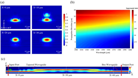
The supermode profile for four different cross-sections along the propagation direction (x) is shown in Fig. 3 (a), for g = 185 nm and λ = 1.55 μm. The supermode dispersion along the adiabatic coupler is shown in Fig. 3 (b), and the normalized electric field distribution along the propagation direction is plotted in Fig. 3 (c), which shows efficient field transfer between the waveguides.
In ON state, in the two narrow sides of the coupler, the supermode index is dominated by the bus waveguide mode index, while in the central part of the coupler (where the moving waveguide is wider than the bus waveguide), the effective index is dominated by the suspended waveguide mode index. As a consequence of the symmetric adiabatic coupler design, the optical power is first coupled to the moving waveguide and then coupled back to the bus waveguide through the coupling length of L = 60 µm. In our design, which is optimized for telecommunication C-band (1530 nm-1565 nm), implementation of the adiabatically tapered waveguide promises a low loss and broadband power transfer between two waveguides. However, during the power transfer, a slight beating of the electric field appears because of the multimode behavior of the adiabatic coupler as it supports two propagating supermodes for the taper widths wider than w(x = 24 µm). In addition, the fringes in electric field distribution which are mainly apparent in the second half of the coupler are originating from interference between the propagating wave and the reflected portion of the light from the waveguide-air facet at the end of the coupler.
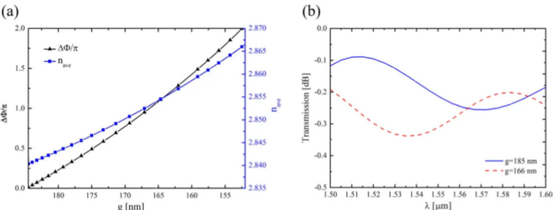
The evolution of the averaged supermode effective index (nave) and the phase shift by the vertical gap for λ = 1.55 μm is shown in Fig. 4 (a). Based on this figure a full π phase shift is applicable by a vertical gap change of Δg = 19 nm which corresponds to 0.165 rad/nm phase shift related to a vertical gap decreasing from g1 = 185 nm to g2 = 166 nm (Δg = 19 nm). This amount of phase shift corresponds to the averaged effective index change of Δneff≈ 0.026 for λ = 1.55 μm. Transmission spectrum of the adiabatic vertical coupler for two vertical gap states g1 = 185 nm and g2 = 166 nm are plotted in Fig. 4 (b) which show a low loss performance over a wide wavelength range with minimum transmission of 95% for λ = 1.55 μm. For a wideband operation, both low loss transmission and minimized phase shift dispersion is desired. For our design the calculated phase shift difference between λ1 = 1.5 μm and λ2 = 1.6 μm is ≈ 0.11π which corresponds to a relatively low phase shift dispersion of 11 × 10−4 π rad/nm. This low dispersion leads to only maximum of ≈ 0.035π phase shift
difference in the telecommunication C-band (1530 nm-1565 nm).
Fig. 3. (a) Normalized profile of the supermode for different locations along the coupler for g = 185nm and λ = 1.55um. (b) Supermode effective index dispersion for g = 185nm. (c) Normalized electric field distribution on y = 0 symmetry plane along the propagation direction. Light transfers between the bus and tapered waveguides with minimum of loss.
When the device is in the OFF state (g = 1 µm) no coupling to the top waveguide is recorded, since simulations show that less than −60 dB is measured in the top waveguide after the first adiabatic taper. The value stays less than −50 dB when the gap is reduced within the stable regime of the first electrostatic actuation (1 µm – 666 nm). The variation of neff is also negligible for this gap range, producing no phase shift. When the gap is ~500 nm the coupling to the top waveguide and neff change start to be detectable, however these positions are not accessible due to the instability of the parallel plate actuator. This behavior highlights also one advantage of the two-step actuator: precise control of the position is achievable in the ON state while allowing sufficiently big displacement between the ON and OFF positions to have no perturbation in the latter state.
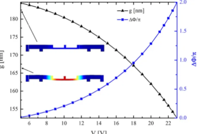
Fig. 4 1.55 µ states 3.2 Mechani To bring the tuning of the mechanism. F first actuation nm. The optim 2 μm × 60 μm series of mech structure to a actuation, the model is used displacement pair in the O stoppers was The outer elec structure is co μm), a comp maintain the flexural defor ensure contro contributes to results of the quadratic dep instability tha parallel plate spring stiffne 185 nm, and cannot be use electrodes do phase delay v previous secti phase shift is total 60 nm an
4. (a) Averaged eff
µm, and (b) the tr
, g1 = 185 nm and
ical and electr
waveguides fr vertical gap in First, we desig n to displace th mized outer sp m) have a pull hanical stoppe set distance fro e pair of inner
d to calculate of the top wav ON state. The optimized to h ctrode sections omposed of a s liant connectio ridge wavegui rmation. The la ol on the wave o the high pull second simula pendence betw at occurs at ar model [30] ssk=340N/ the electrode ed in this case
not stay paral versus the wav ion, we can ca
achievable wit nd 30.1 V give
fective index and t ransmission spectr
g2 = 166 nm.
rostatic
from OFF state n ON state, w gned the folded
he device into prings (stiffness l-in voltage (V rs with a preci om the outer e r electrodes is the response o veguide and to e connection b have high stiff s are stable in O tiff connection on section and ide parallel to ack of deforma eguides separa l-in voltage of ation. We find ween the appl round 1/3 of predicts the p m , extracted f areaA=2×1.
e to evaluate p lel to the botto veguide separa alculate the tot
thin 33 nm of d en by the pull-in
the relative phase rum of the phase
e to the coupl we implement a d spring struct the ON state a s equivalent to Vpi) of 4 V. At ise height of 1 lectrodes in th used to tune of the structur verify the mec between the o fness in order t ON-state up to n section, a pai d the ridge w the bottom bu ation in the tap ation and thus f the second ac a behavior sim lied voltage a
the initial sep pull-in atVpi = from the nume
.5 μm×60 μm
recisely the re om ones when ation from the tal phase shift displacement a n instability.
shift versus the v shifter in two dis
led ON state, a parallel plate tures and the o and reduce the o 0.2 N/m) and each side of t 85 nm are plac he ON-state (se
the waveguide re after the firs chanical stabili outer electrode to avoid collap 94 V before p ir of inner elect waveguide. The us waveguide pered ridge wa the phase shi ctuator (30.1 V milar to a parall
and the displa paration betwe 2 1 0 (8kd /27εA) = erical simulati . However, th esponse of the increasing the e optical simu
versus the app and 23 V of app
vertical gap for λ = stinct vertical gap
as well as for e electrostatic outer electrode e waveguide ga d pair of electro these outer ele ced to keep the ee Fig. 2). Afte
e separation. A st pull-in to ex ity of the first es and the m pse of the top pull-in occurs. T
trodes (2 × 1.5 e compliant co
by yielding th aveguide is imp ifting. The stif V). Figure 5 s lel plate actuat acement with een the electro 1/ 2 31.5 V , u ion, the initial he parallel pla structure sinc e voltage. By f ulation describe plied voltage. A plied voltage, o = p r the fine actuation es for the ap to 185 odes (2 × ectrodes a e moving er the first A second xtract the electrode echanical structure. The inner 5 μm × 60 onnectors he largest portant to ff section shows the tor with a a pull-in odes. The using the gap g1 = ate model ce the top fitting the ed in the A full 2π out of the
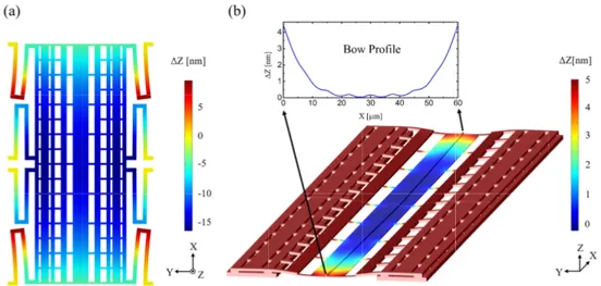
Fig. 5 the ex maxim So far we models using due to stress. compressive deposited by appropriate an difference in mechanical po negligible. Th aligned to the 6(b) shows th We verify th values of 400 part along the electrostatic f suspended str cut-line along material stres nm when the waveguide ca part of the tap L/2 = 30 µm simulations fo difference of waveguide su overall small
. Vertical gap and xaggerated deform mum deformation) e neglected the only solid me . In Fig. 6(a) stress of 400 M y chemical va nnealing techn n waveguide s olishing (CMP he folded sprin e bottom bus w he simulation o he effect of the 0 MPa, 200 MP e propagation d force and it is ructure that cau g the center of s accentuates device operate auses maximum pered waveguid m, thus it has or a configurat less than 0.1% ubject to displa neff change.
d phase shift versu mation for two de ). e intrinsic stre echanics physi the deformatio MPa, consider apor depositio niques. The ma separation is P) on the design ngs and the sy waveguide whe f the ON state e stress in thi Pa and 0 Pa. In direction can b s due to the ta uses a reductio f the tapered w the amount of es in stable equ m vertical gap de. Note that th
not any consi tion with the m % in comparison
acement is wh
s bias voltage at th efined vertical ga
ss of the poly ics were used on induced by red a maximum on, which can aximum resultin lower than th ned gap, theref ymmetric desi en intrinsic str with the electr is configuratio n all three case be observed. T apering of the on of the mecha waveguide is d f bowing, but t uilibrium (befo difference of 4 his gap differen iderable effect mentioned bow n with the bow en the width o he inner electrodes aps (blue = no de ysilicon layer. to assess any y the stress is m stress value n typically fu ng deflection a he uncertainty fore the effect ign maintain t ress is present rostatic force a on by using th es a bowing of The bowing inc waveguide to anical stiffness depicted in ins the increase st re pull-in). Th 4.5 nm betwee nce happens fo t on the overa wing leads to a w-less structure of the ridge is
s. The insets show eformation, red = Separate finite parasitic displ shown. We as e for typical po further be red amounts to 10 y caused by on the first ac the suspended in the materia acting on the el hree compressi f the tapered w creases with th owards the en s. The bow pro set of Fig. 6(b tays in the ran e bowing of th en narrow part or propagation all phase shift a negligible ph e. Indeed, the p smallest, prod w = e element lacements ssumed a olysilicon duced by nm. This chemical ctuation is structure al. Figure lectrodes. ive stress waveguide he applied ds of the ofile for a ). Higher nge of 0.2 he tapered and wide length of t. Optical hase shift part of the ducing an
Fig. 6 and n symm field electro of cro waveg The desig separately. Fo 10 V) and inn connectors ar state, it is also OFF the devic A source thermomecha operates out 4 B x k T < >= the mechanica of mechanica estimate < >x 4. Simulatio Optical simul by Lumerical 2 nm precisio order to obtain network in the simulation are one output po entire simula reflection fro method (FEM simulations w to calculate th used to calcul
6. (a) Vertical com no electrostatic fo metric structure and
with 400 MPa c odes pair. The wa oss section. Inset guide. Deformatio
gn as presented or this scheme, ner electrode st round the oute o possible to sh ce (0 V-10 V)
of noise cou anical noise, sin of resonanc 3 m T Qmω , wh al quality facto al simulations 0.3 pm/ H > ons method lations were pe . The supermo on in meshing n the transmiss e coupler’s cro ea included on ort to monitor ation domain m the bounda M) models to ca were performed he tapered wav late the respon
mponent of the disp rce. The top wav d the use of folded compressive mate aveguide bows alo t shows the bow
n is exaggerated.
d assumes tha , a digital ON-teps from 0 V t er electrodes h hort the two el and then increa uld be the flu nce the phase ce, the fluctu here kB is the B
or, m the mass and from the
Hz, correspond
erformed using de effective in and the perfe sion spectra, 3D oss-section and
e input port to the transmissi was surrounde aries into the s alculate the pu d in COMSOL veguide displac se of the struct placement with 40 veguide has no in d springs. (b) Vert erial stress and e ong the propagatio profile for a cu
at the inner an -OFF signal is to 19 V to achi have been dim lectrodes pair a ase it from 10 V uctuation of t shift is very s uation of the Boltzmann con and ωm the me characterizati ding to a phase g the finite diff ndex is calculat ctly matched l D FDTD Solut d 50 nm mesh s launch the bus ion and calcul ed by the per simulation dom ull-in voltage o L Multiphysics
cement with th ture after the fi
00 MPa compressi n-plane displacem tical component of electrostatic force on direction cause ut-line along cent
nd outer electr applied to the ieve π phase sh mensioned to av and use a sing V to 20 V to o the top wave sensitive to the e gap can b nstant, T the a echanical reson ion of similar difference of Δ fference time d ted using FDT layer (PML) b tions was empl steps in the pro s waveguide’s late the optical rfectly matche main. We con of the first and using the elec he applied volt first pull-in to e
ive material stress ment thanks to the f the displacement applied on both ed by the variation ter of the tapered
rodes can be c e outer electrod hift. However, void pull-in in gle signal to sw obtain π phase s eguide position e gap. Since th e expressed ambient tempe nance. Using th structures [8] 5 10 π − ΔΦ × domain (FDTD TD Mode Solut boundary cond loyed with a 5 opagation direc fundamental m l mode expans ed layers to o nstructed finite second actuat ctromechanics age. A second extract the disp
s e t h n d controlled des (0 V-since the n the ON witch ON-shift. n due to he device as [31]: erature, Q he results ], we can . D) method tions with ditions. In nm mesh ction. The mode and sion. The omit any e element tions. The interface d model is placement
of the top waveguide and to verify the mechanical stability of the first electrode pair in the ON state. In the second model, the folded springs are replaced by the resulting restoring force and spring foundation as boundary conditions. The contact between the suspended structure and the substrate is modelled with a roller boundary condition at the polysilicon mechanical stoppers.
5. Conclusion
We propose a design for an analog Silicon Photonic MEMS-based phase shifter with a low loss and broadband performance over the telecommunication C-band. The phase shifter includes a vertical adiabatic coupler composed of fixed and vertically movable waveguides. The symmetrically tapered 60 µm long vertically moving waveguide is actuated in two steps using two pairs of electrodes following the parallel plate electrostatic actuation mechanism to approach the fixed bus waveguide and consequently modify the signal phase. Numerical simulations are used for performance evaluation. The phase shifter turns ON by applying 4 V to the first pair of the electrodes leading to their pull-in and bringing the waveguides to a well-controlled 185 nm of vertical gap. In the ON state a full π phase can be achieved by decreasing the gap by 19 nm, by applying 19 V to the inner set of the electrodes. The two sets of soft and stiff springs lead to a robust design against stress related failure mechanisms as well as the pull-in instability in ON state. FDTD simulations predict an average insertion loss at a full period phase shift in the C-band below 0.3 dB. The design is entirely compatible with previously demonstrated surface micromachined Silicon Photonic MEMS manufacturing process, occupies a total footprint of merely 60 μm × 40 μm and can serve as an efficient building block for MEMS-based reconfigurable Silicon Photonic integrated circuits.
Funding
Hasler Stiftung Foundation (Grant No. 17008), Swiss National Science Foundation (Grant No. 157566).
References
1. J. Bryzek, S. Roundy, B. Bircumshaw, C. Chung, K. Castellino, J. R. Stetter, and M. Vestel, “Marvelous MEMS,” IEEE Circuits and Devices Magazine 22(2), 8–28 (2006).
2. A. E. Lim, J. Song, Q. Fang, C. Li, X. Tu, N. Duan, K. K. Chen, R. P. Tern, and T. Liow, “Review of silicon photonics foundry efforts,” IEEE J. Sel. Top. Quantum Electron. 20(4), 405–416 (2014).
3. A. Rickman, “The commercialization of silicon photonics,” Nat. Photonics 8(8), 579–582 (2014). 4. N. Quack, T. J. Seok, S. Han, H. Sattari, T. Graziosi, M. Kiss, R. S. Muller, and M. C. Wu, “Surface
micromachined silicon photonic MEMS: a scalable technology platform for photonic network components,” in
Advanced Photonics 2018 (BGPP, IPR, NP, NOMA, Sensors, Networks, SPPCom, SOF) (2018), Paper NeM4F.1
(Optical Society of America, 2018), p. NeM4F.1.
5. B. Abasahl, I. Zand, C. Lerma Arce, S. Kumar, N. Quack, M. A. Jezzini, H. Y. Hwang, K. B. Gylfason, M. G. Porcel, and W. Bogaerts, “Towards low-power reconfigurable photonic ICs based on MEMS technology,” in Australian Institute of Physics Congress (2018).
6. J. Capmany, I. Gasulla, and D. Pérez, “The programmable processor: Microwave photonics,” Nat. Photonics
10(1), 6–8 (2016).
7. “Birth of the programmable optical chip,” Nat. Photonics 10(1), 1 (2016).
8. T. J. Seok, N. Quack, S. Han, R. S. Muller, and M. C. Wu, “Large-scale broadband digital silicon photonic switches with vertical adiabatic couplers,” Optica, OPTICA 3(1), 64–70 (2016).
9. T. Liu, F. Pagliano, and A. Fiore, “Nano-opto-electro-mechanical switch based on a four-waveguide directional coupler,” Opt. Express 25(9), 10166–10176 (2017).
10. Q. Xu, L. Chen, M. G. Wood, P. Sun, and R. M. Reano, “Electrically tunable optical polarization rotation on a silicon chip using Berry’s phase,” Nat. Commun. 5(1), 5337 (2014).
11. D. T. Fuchs, H. B. Chan, H. R. Stuart, F. Baumann, D. Greywall, M. E. Simon, and A. Wong-Foy, “Monolithic integration of MEMS-based phase shifters and optical waveguides in silicon-on-insulator,” Electron. Lett. 40(2), 142–143 (2004).
12. C. Errando-Herranz, M. Colangelo, S. Ahmed, J. Björk, and K. B. Gylfason, “MEMS tunable silicon photonic grating coupler for post-assembly optimization of fiber-to-chip coupling,” in 2017 IEEE 30th International
13. T. Graziosi, H. Sattari, T. J. Seok, S. Han, M. C. Wu, and N. Quack, “Silicon photonic MEMS variable optical attenuator,” in MOEMS and Miniaturized Systems XVII (International Society for Optics and Photonics, 2018),
10545, p. 105450H.
14. H. Sattari, A. Toros, T. Graziosi, and N. Quack, “Bistable silicon photonic MEMS switches.” in MOEMS and
Miniaturized Systems XVIII (International Society for Optics and Photonics, 2019), 10931, p. 109310D.
15. J. Carolan, C. Harrold, C. Sparrow, E. Martín-López, N. J. Russell, J. W. Silverstone, P. J. Shadbolt, N. Matsuda, M. Oguma, M. Itoh, G. D. Marshall, M. G. Thompson, J. C. F. Matthews, T. Hashimoto, J. L. O’Brien, and A. Laing, “Universal linear optics,” Science 349(6249), 711–716 (2015).
16. M. H. Khan, H. Shen, Y. Xuan, L. Zhao, S. Xiao, D. E. Leaird, A. M. Weiner, and M. Qi, “Ultrabroad-bandwidth arbitrary radiofrequency waveform generation with a silicon photonic chip-based spectral shaper,” Nat. Photonics 4(2), 117–122 (2010).
17. J. Sun, E. Timurdogan, A. Yaacobi, E. S. Hosseini, and M. R. Watts, “Large-scale nanophotonic phased array,” Nature 493(7431), 195–199 (2013).
18. A. Liu, L. Liao, D. Rubin, H. Nguyen, B. Ciftcioglu, Y. Chetrit, N. Izhaky, and M. Paniccia, “High-speed optical modulation based on carrier depletion in a silicon waveguide,” Opt. Express 15(2), 660–668 (2007).
19. N. C. Harris, Y. Ma, J. Mower, T. Baehr-Jones, D. Englund, M. Hochberg, and C. Galland, “Efficient, compact and low loss thermo-optic phase shifter in silicon,” Opt. Express 22(9), 10487–10493 (2014).
20. A. Melikyan, L. Alloatti, A. Muslija, D. Hillerkuss, P. C. Schindler, J. Li, R. Palmer, D. Korn, S. Muehlbrandt, D. Van Thourhout, B. Chen, R. Dinu, M. Sommer, C. Koos, M. Kohl, W. Freude, and J. Leuthold, “High-speed plasmonic phase modulators,” Nat. Photonics 8(3), 229–233 (2014).
21. J. Henriksson, T. J. Seok, J. Luo, K. Kwon, N. Quack, and M. C. Wu, “Digital silicon photonic mems phase-shifter,” in 2018 International Conference on Optical MEMS and Nanophotonics (OMN) (2018), pp. 1–2. 22. M. W. Pruessner, D. Park, T. H. Stievater, D. A. Kozak, and W. S. Rabinovich, “Broadband
opto-electro-mechanical effective refractive index tuning on a chip,” Opt. Express 24(13), 13917–13930 (2016).
23. M. Poot and H. X. Tang, “Broadband nanoelectromechanical phase shifting of light on a chip,” Appl. Phys. Lett.
104(6), 061101 (2014).
24. W. C. L. Hopman, K. O. van der Werf, A. J. Hollink, W. Bogaerts, V. Subramaniam, and R. M. de Ridder, “Nano-mechanical tuning and imaging of a photonic crystal micro-cavity resonance,” Opt. Express 14(19), 8745–8752 (2006).
25. P. T. Rakich, M. A. Popovic, M. R. Watts, T. Barwicz, H. I. Smith, and E. P. Ippen, “Ultrawide tuning of photonic microcavities via evanescent field perturbation,” Opt. Lett., OL 31(9), 1241–1243 (2006).
26. H. Sattari, T. Graziosi, M. Kiss, T. J. Seok, S. Han, M. C. Wu, and N. Quack, “Analog Silicon Photonic MEMS phase-shifter with double-step electrostatic actuation,” in 2017 International Conference on Optical MEMS and
Nanophotonics (OMN) (IEEE, 2017), pp. 1–2.
27. A. Hardy and W. Streifer, “Coupled mode theory of parallel waveguides,” J. Lightwave Technol. 3(5), 1135– 1146 (1985).
28. X. Sun, H.-C. Liu, and A. Yariv, “Adiabaticity criterion and the shortest adiabatic mode transformer in a coupled-waveguide system,” Opt. Lett., OL 34(3), 280–282 (2009).
29. A. L. Hartzell, M. G. da Silva, and H. R. Shea, “Lifetime prediction,” in MEMS Reliability, A. L. Hartzell, M. G. da Silva, and H. R. Shea, eds., MEMS Reference Shelf (Springer US, 2011), pp. 9–42.
30. G. N. Nielson and G. Barbastathis, “Dynamic pull-in of parallel-plate and torsional electrostatic MEMS actuators,” J. Microelectromech. Syst. 15(4), 811–821 (2006).
31. A. N. Cleland, Foundations of Nanomechanics : From solid-state theory to device applications, advanced texts in physics (Springer, 2003).