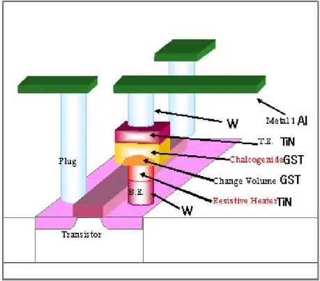
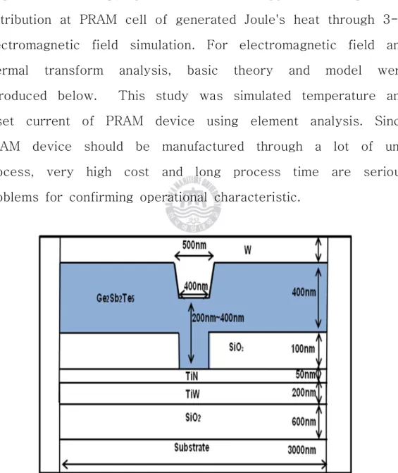
본 논문에서는 차세대 메모리인 상변화 메모리의 소거 전류를 줄이기 위한 셀 구조의 새로운 랜덤 액세스 메모리에 대해 기술한다. 특히 상변화 물질을 히터로 사용하는 Pore-type PRAM은 리셋 전류를 줄이는 데 관심이 쏠렸다. 칼코겐화물은 주기율표의 산소/황 계열(새 스타일의 16족 또는 기존 주기율표의 VI족)의 원소를 포함하는 합금입니다.
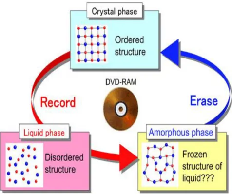
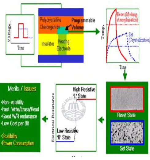
Cooler parts of the chalcogenide take longer to crystallize and superheated parts can remelt[8]. In PRAM, we are exploiting the difference in resistance between the two material phases. This phase change is induced in the material through intense localized Joule heating caused by current injection[17, 18].
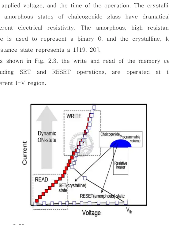
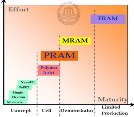
The final phase of the material is modulated by the magnitude of the injected current. 2.3, the writing and reading of the memory cell, including SET and RESET operations, are performed in the different I-V regions. PRAM (Phase Change Random Access Memory) is one of the most promising candidates for next-generation non-volatile memories because PRAM combines all the desirable features such as DRAM, Flash and SRAM.
For PRAM, phase change material Ge2Sb2Te5 (GST) is transformed to crystalline (SET) or amorphous (RESET) state by applied current.
Poisson's equation is,
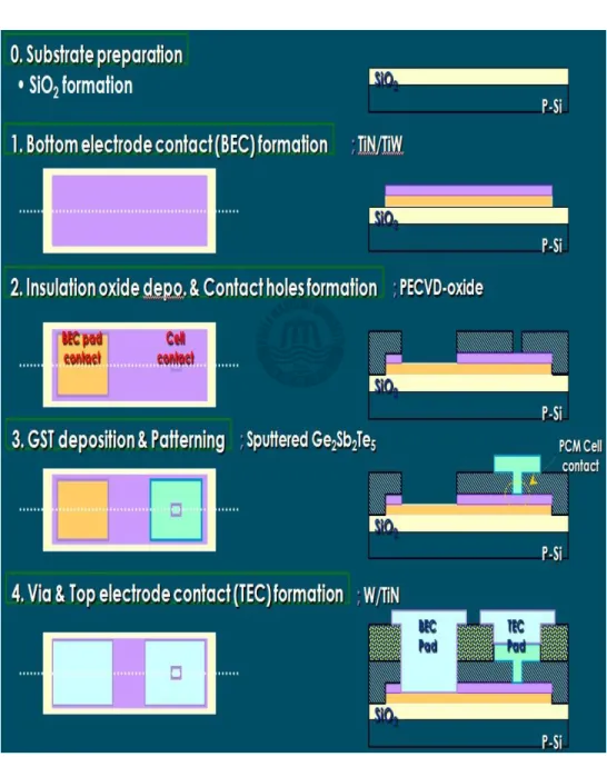
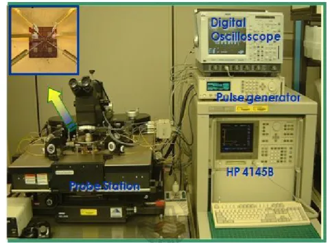
Experimental
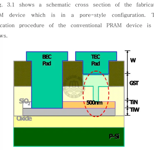
Oxide
BEC BEC
Pad Pad TEC TECPad
TiW TiWTiNTiN
SiOSiO 2 2
Results and discussion
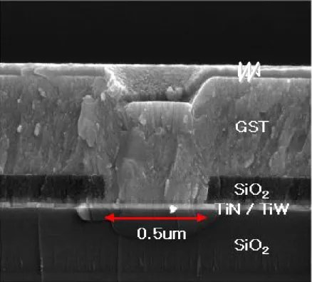
Using a 3-D finite element analysis tool, we investigated the temperature and reset current of a PRAM unit cell with the thickness of a GST nanoscale PRAM thin film. To reduce the reset current, we proposed a new PRAM unit cell structure with heat blocking layer and investigated the electro-thermal properties of high density PRAM with heat blocking layer. The GST film was successfully integrated into the pore-type unit cell without processing problems.
And we investigated the electrical characteristics of PRAM unit cells using fabricated pore-type PRAM unit cells. First, we analyzed the temperature distribution of the PRAM unit cell by resetting the current to test the reliability of commercial electrothermal analysis tools used in simulation. As the reset current is applied to the constructed PRAM cell model, heat is transferred to phase change material.
As the thickness of the GST film was thinned from 400 ㎚ to 300 ㎚, the reset current increased slightly, but did not affect the performance of the memory cells as much. But as the thickness of the GST thin film became as thin as 300㎚ and 150㎚, the reset current suddenly increased and the operation of the memory cell did not work normally. In this figure, the reset current is that the right reset current can melt the phase change material to the amorphous state.
Therefore, we have thoroughly investigated the malfunction of PRAM unit cell with a thickness of 200㎚ GST. We have investigated the reason why the temperature decreased and the reset current increased as the thickness of GST became thin. A heat which came into contact with the upper electrode is easily transferred to the outside, and the temperature decreased and the reset current increased.
The proposed new PRAM unit cell structure deposited SiO2 as a blocking layer between the top electrode and the phase change material. The power (ohmic loss) of GST thin film is greatly increased compared to conventional PRAM. 4.11 (a) shows that the reset current of the conventional structure flowed from the top electrode to the bottom electrode through the center of the GST thin film.
But, in a new structure, you reset the current from the outside of the SiO2. blocking layer to the bottom electrode, as shown. Fig. b) New PRAM unit cell structure. Fig. However, in the planar type PRAM unit cell, heat is generated between GST and the bottom electrode contact.
Bottom electrode
After using SiO2 heat blocking layer, we got good effect on pore type PRAM cell.
Top electrode GST
Top electrode
Conclusion
Due to the increasing costs of scaling back Flash technology, the memory industry is looking for an alternative memory concept. In this paper, we fabricated the PRAM unit cell and investigated the electrical and thermal properties of a PRAM unit cell with a new structure using the SiO2 heat blocking layer. When the thickness of the GST thin film decreased from 400 ㎚ to 300 ㎚, the reset current and temperature changed a little, but it did not affect the operation of the memory cell.
As the reset current and temperature changed as at 200 thickness of GST thin film, the memory cell did not function. From these results, we investigated material parameters of heater electrode for why the reset current and temperature changed. After investigation, we found that heat generated between phase change material GST and heater electrode TiN was given to upper electrode W due to thin thickness of GST thin film.
In the case of 200 ㎚ thickness of GST thin film, heat is quickly transferred to the top electrode before the melting temperature. The SiO2 blocking layer, which is a dielectric layer, can protect the heat emitted through the upper electrode. Compared with the conventional PRAM at 200nm GST thin film thickness, the PRAM temperature of the new structure increased sharply from 536.60℃ to 817℃, and the reset current of the PRAM of the new structure decreased suddenly.
This result shows that the new SiO2 blocking layer of PRAM successfully shielded heat from emitting to the top electrode.
7] Marcus Yam, Intel will try Phase Change Memory this year via the website www.dailytech.com. 12] M.Gill et al., "Ovonic Unified Memory - A high performance non-volatile memory technology for stand alone memory and embedded applications." Proceedings of the ISSC.