Vol. 67, No. 3, March 2017, pp. 283∼288 http://dx.doi.org/10.3938/NPSM.67.283
Study of the Characteristics of a Schottky Diode Prepared by Using Ag on Mg
xZn
1−xO Films with a Mg Content
Lili Yue · Hong Seung Kim
∗Department of Electronic Material Engineering, Korea Maritime and Ocean University, Busan 49111, Korea
Nak Won Jang
Division of Electrical and Electronics Engineering, Korea Maritime and Ocean University, Busan 49111, Korea
Young Yun
Division of Radio Communication Engineering, Korea Maritime and Ocean University, Busan 49111, Korea (Received 22 June 2016 : revised 25 October 2016 : accepted 27 October 2016)
We investigated lateral Schottky diodes based on MgxZn1−xO (0 ≤ x ≤ 0.18) films with sil- ver (Ag) Schottky metals. The MgxZn1−xO films were deposited on Si substrates by using RF magnetron co-sputtering with ZnO and Mg0.3Zn0.7O targets. The Mg contents were controlled by using the power on the Mg0.3Zn0.7O target. The electrical properties of Schottky diodes based on MgxZn1−xO films with Ag metal as functions of the Mg content were discussed. The Ag Schottky diode based on the Mg0.18Zn0.82O film exhibited rectification ratios as high as∼103at a bias voltage of±1 V, with an ideality factor of 1.68 and a Schottky barrier height of 0.73 eV.
PACS numbers: 61.66.Fn, 72.80.Ey, 81.40.Ef, 81.15.Cd
Keywords: Schottky diode, MgxZn1−xO, Mg content, Ag contact, RF magnetron co-sputtering
I. INTRODUCTION
Zinc oxide (ZnO) has been attracted to apply of opto- electronic devices, gas and chemical sensors, and tran- sistors [1–3], because of the wide band-gap (3.37 eV) compound semiconductor with the large exciton binding energy (60 meV). Recently, ternary MgxZn1−xO, that is one type of ZnO alloys, in particular, has strongly paid attention for the application in deep-ultraviolet op- toelectronic devices [4,5]. Because the energy band gap of MgxZn1−xO is able to tailor from 3.37 eV to 7.8 eV with Mg content, it can cover a wide range of the deep- ultraviolet spectrum. Furthermore, the MgxZn1−xO has the high resistance to radiation, the handiness to conven- tional wet etching, the environmental and bio friendly characters, and the low deposition temperatures.
∗E-mail: [email protected]
A metal/semiconductor Schottky junction is very use- ful for evaluating the fundamental electronic properties of semiconductors [6]. The metals with large work func- tion such as Pt (Φ = 5.65 eV), Au (Φ = 5.1 eV), Ag (Φ
= 4.26 eV), and Pd (Φ = 5.12 eV) have been used as Schottky contacts to ZnO. The ZnO film based Schot- tky diodes have been widely investigated and several surface pretreatment methods, such as oxygen plasma treatment and hydrogen peroxide (H2O2) treatments, have been proposed to improve the Schottky proper- ties by reducing the surface defects [6]. However, the study of MgxZn1−xO based Schottky diode is very lim- ited. Yoon et al. [7] investigated the indium tin oxide (ITO) Schottky contacts on MgZnO/ZnO heterostruc- tures. The barrier height between ITO and MgZnO/ZnO is 0.61 eV and its ideality factor is 4.1. Mohanta et al. [8] studied the Pt Schottky diode based on H2O2
treated MgZnO:N films and resulted in a relatively good Schottky properties with the ideality factor of 2.79 and
This is an Open Access article distributed under the terms of the Creative Commons Attribution Non-Commercial License (http://creativecommons.org/licenses/by-nc/3.0) which permits unrestricted non-commercial use, distribution, and reproduction in any medium, provided the original work is properly cited.
284 New Physics: Sae Mulli, Vol. 67, No. 3, March 2017
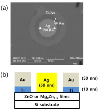
Fig. 1. (Color online) (a) SEM image showing a top view of the lateral Schottky diode pattern and (b) a schematic cross section of the Schottky diode.
Schottky barrier height of 0.69 eV. To expand the appli- cation of MgxZn1−xO film in deep-ultraviolet optoelec- tronic devices, both high quality MgxZn1−xO film and good electricity of metal/MgxZn1−xO Schottky contact are needed.
In this work, we describe the Schottky contact prop- erties of Ag in contact with MgxZn1−xO (0≤ x ≤ 0.18) films on Si substrates without surface treatment. The effect of Mg content on electrical properties of Schottky diodes based on MgxZn1−xO (0≤ x ≤ 0.18) films with Ag metal was investigated. The MgxZn1−xO films were deposited by RF magnetron co-sputtering with ZnO and Mg0.3Zn0.7O targets.
II. EXPERIMENT
We used the RF magnetron co-sputtering that in- stalled the co-sputtered commercial targets, ZnO and Mg0.3Zn0.7O (4 inch in diameter, Mg/(Mg+Zn), 30 at.%), with purity of 99.99% to deposit MgxZn1−xO films on n-Si (100) substrates. Before loading, the substrates were simply cleaned in order of acetone, methanol, and de-ionized water in an ultrasonicator for 15 min. The working chamber conditions are the base
Fig. 2. (Color online) XRD θ-2θ patterns for ZnO, Mg0.02Zn0.98O, Mg0.11Zn0.89O, Mg0.18Zn0.82O, and Mg0.3Zn0.7O films.
pressure of lower than 10−6 Torr, the working pressure of 5 mTorr, and argon gas flow rate of 20 cm3/min. And all of the ZnO and MgxZn1−xO films were deposited for 90 min at 300 ◦C. The RF power of ZnO target fixed at 100 W, while the applied power of Mg0.3Zn0.7O tar- get was changed to 0 W, 50 W, 100 W, and 150 W.
According to the applied power of Mg0.3Zn0.7O target, the corresponding samples were labeled as ZnO, MZO50, MZO100, and MZO150, respectively.
After deposition, a lateral Schottky diode in Fig. 1 was fabricated by photolithography that was set up of our previous work [9]. The annular Ti (10 nm)/Au(50 nm) ohmic rings in Fig. 1(a) which were deposited by electron beam (e-beam) evaporation was formed by lift- off photolithography. To form ohmic contacts the Ti/Au contact metals were post-annealed at 300 ◦C in vacuum for 3 min by rapid thermal process. Then the inner circle of Ag (50 nm) Schottky contact was fabricated by lift- off photolithography and e-beam evaporation. Fig. 1(b) shows the schematic cross section of the fabricated de- vices.
The Mg concentration was measured by energy dis- persive X-ray analysis (EDAX, Tescan, MIRA-3). The structural properties were characterized by the X-ray diffraction (XRD, Rigaku, Smartlab). The electrical properties and the current-voltage (I − V ) character- istics were investigated by a Hall effect measurement (Ecopia, HMS-5000) and a semiconductor parameter analysis (Hewlett-Packard, HP-4145B).
Fig. 3. (Color online) I−V characteristics of Ag Schottky contacts on (a) ZnO, (b) Mg0.02Zn0.98O, (c) Mg0.11Zn0.89O, and (d) Mg0.18Zn0.82O films. The inserted figure shows the I− V characteristics between Ti/Au contacts on the ZnO and MgxZn1−xO films.
III. RESULTS AND DISCUSSION
A top-view of the SEM image of the patterned Schot- tky diode can be shown in Fig. 1(a). The diameter of the Shottky contact is 200 µm and the distance from the Shottky contact to ohmic contact is 60 µm. The inner circle pattern was formed Schottky contacts by Ag, while outer ring was formed ohmic contacts by Ti/Au metal on the MgxZn1−xO films.
The Mg concentration of MgxZn1−xO films was con- firmed by EDAX spectrum. Mg compositions of MZO50, MZO100, and MZO150 are 2 at.%, 11 at.%, and 18 at.%, respectively. The Mg content increases as the power of Mg0.3Zn0.7O target increases. Fig. 2 shows the XRD diffraction patterns of ZnO, Mg0.02Zn0.98O, Mg0.11Zn0.89O, and Mg0.18Zn0.82O films. All sam- ples predominantly show (002) direction with hexago- nal wurtzite structure and that is no phase separation.
The ZnO (002) diffraction peak is 34.3◦ whereas the Mg0.02Zn0.98O, Mg0.11Zn0.89O, and Mg0.18Zn0.82O films display hexagonal MgZnO (002) peaks at 34.3◦, 34.34◦, and 34.38◦, which shifts to the 34.44◦observed for single Mg0.3Zn0.7O target. This indicates an increase in the incorporation of Mg into ZnO, which is consistent with the EDAX result.
Fig. 3 shows the I − V (black square-dotted line) curves which were measured at room temperature in dark, and the log|I|−V (red triangle-dotted line) curves of the Schottky diodes based on ZnO, Mg0.02Zn0.98O, Mg0.11Zn0.89O, and Mg0.18Zn0.82O films with Ag Schot- tky metal. For a Schottky diode, current transport is due to majority carriers and it is described by the thermionic emission over the interface barrier. The equation of the diode can be written as [10]
I = I0 [
exp(q(V − IRS) nkT )− 1
]
(1)
286 New Physics: Sae Mulli, Vol. 67, No. 3, March 2017
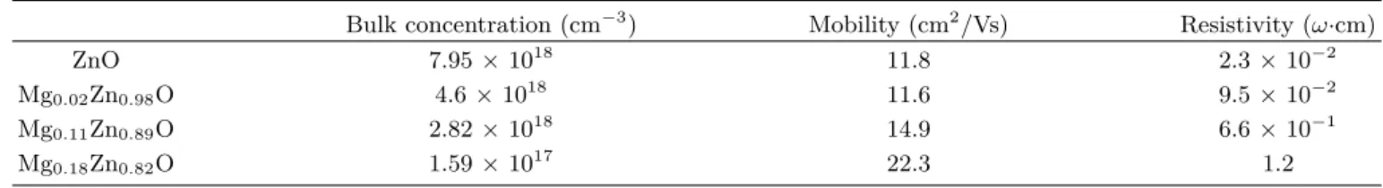
Table 1. Electrical properties of MgxZn1−xO films measured by Hall effect measurement.
Bulk concentration (cm−3) Mobility (cm2/Vs) Resistivity (ω·cm)
ZnO 7.95× 10¹⁸ 11.8 2.3× 10⁻²
Mg0.02Zn0.98O 4.6× 10¹⁸ 11.6 9.5× 10⁻²
Mg0.11Zn0.89O 2.82× 10¹⁸ 14.9 6.6× 10⁻¹
Mg0.18Zn0.82O 1.59× 10¹⁷ 22.3 1.2
where I0 is the saturation current, q is the electron charge, n is the ideality factor, k is the Boltzmann con- stant, RS is the series resistance, and T is the absolute temperature.
Fig. 3(a) shows the I − V curve of the Ag Schot- tky diode fabricated on ZnO film. As the voltage in- creases, the current increases linearly. This is because that ZnO film displays a higher carrier concentration of 7.95 × 10¹⁸/cm3 than MgxZn1−xO (0.02 ≤ x ≤ 0.18) films, as shown in Table 1, which were measured by Hall effect measurement at room temperature. The metal contact on a high-carrier-density material can be form an ohmic contact owing to tunneling current transport process [11]. Figs. 3(b), (c), (d) show the I− V and log|I|−V curves of the Ag Schottky diodes fabricated on Mg0.02Zn0.98O, Mg0.11Zn0.89O, and Mg0.18Zn0.82O films.
The inserted figures show the I − V characteristics be- tween Ti/Au contacts on MgxZn1−xO thin films, which verify the good ohmic contact properties. These de- vices show clear rectification behavior, with turn-on volt- ages of 0.31 V (Mg0.02Zn0.98O), 0.32 V (Mg0.11Zn0.89O), and 0.5 V (Mg0.18Zn0.82O). The leakage currents of the Schottky diodes at a voltage of -1 V are 3.21 × 10⁻⁴ A (Mg0.02Zn0.98O), 1.22 × 10⁻⁵ A (Mg0.11Zn0.89O), and 5.11 × 10⁻⁹ A (Mg0.18Zn0.82O) at room temperature.
The forward current (IF)/reverse current (IR) ratios of the Schottky diodes at ±1 V are 2.10 (Mg0.02Zn0.98O), 2.04 (Mg0.11Zn0.89O), and 2.25× 10³ (Mg0.18Zn0.82O).
The Ag/Mg0.18Zn0.82O Schottky diode shows the highest rectifying ratio.
The diode ideality factor (n) can be determined from the slope of semi-logarithmic forward bias I–V plot for 0.25>V >3 kT/q. The ideality factor of Mg0.02Zn0.98O, Mg0.11Zn0.89O, and Mg0.18Zn0.82O based Schottky diodes with Ag metal are 4.81, 4.66, and 1.68, respec- tively. The n ≥ 2 indicates that thermionic emission is no longer the dominant transport mechanism. In other
words this behavior is often attributed to defect states in the band gap of the semiconductor providing other cur- rent transport mechanisms such as barrier tunneling or generation-recombination in the space charge region [12].
High ideality factors have also been attributed to later- ally inhomogeneous contacts caused by nonuniformities in the Schottky interface, such as structural defects, sur- face contamination, and variations in interface compo- sition [12]. According to the Hall effect measurement results as shown in Table 1, the carrier concentrations of Mg0.02Zn0.98O, Mg0.11Zn0.89O, and Mg0.18Zn0.82O are 4.6 × 10¹⁸ /cm3, 2.82 × 10¹⁸ /cm3, and 1.59 × 10¹⁷ /cm3, which decreases as the Mg concentration increases.
This indicates that the incorporation of Mg into ZnO re- duces the formation of oxygen vacancies which acting as donors for electrons below the contact. So the ideality factor decreases as the Mg concentration increases. The Ag/Mg0.18Zn0.82O Schottky diode displays the lowest n value of 1.68.
The Schottky barrier height was calculated as [13]
I0= AA∗T2exp (
−qΦB kT
)
(2)
where ΦB is the barrier height, A is the area of the diode, and A∗ is the effective Richardson constant. I0
can be derived from the straight-line intercepts of the ln|I| − V curves when applied voltage is zero. If the ef- fective Richardson constant of a material is known, ΦB
can be deduced from Eq. (2). But, the value of A∗ for MgZnO has not been reported, so, we used the value of ΦBof ZnO that is 32 Acm−2K−2to calculate the barrier height. The ΦBvalues of Mg0.02Zn0.98O, Mg0.11Zn0.89O, and Mg0.18Zn0.82O based Schottky diodes with Ag metal are 0.47 eV, 0.55 eV, and 0.73 eV, which increases with the increasing in Mg concentration. Perkins et al. [14] re- ported that the incorporation of Mg into ZnO moves the conduction band minimum of ZnO up in energy. That is, the electron affinity (χs) of MgxZn1−xO decreases as
Fig. 4. (Color online) I/(dI/dV ) vs. current for the (a) Ag/Mg0.02Zn0.98O, (b) Ag/Mg0.11Zn0.89O, and (c) Ag/Mg0.18Zn0.82O Schottky diode.
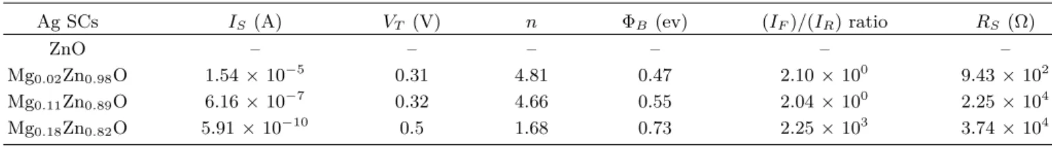
Table 2. Electrical properties of MgxZn1−xO films measured by Hall effect measurement
Ag SCs IS (A) VT (V) n ΦB (ev) (IF)/(IR) ratio RS (Ω)
ZnO – – – – – –
Mg0.02Zn0.98O 1.54× 10⁻⁵ 0.31 4.81 0.47 2.10× 100 9.43× 10²
Mg0.11Zn0.89O 6.16× 10⁻⁷ 0.32 4.66 0.55 2.04× 100 2.25× 10⁴
Mg0.18Zn0.82O 5.91× 10⁻¹⁰ 0.5 1.68 0.73 2.25× 10³ 3.74× 10⁴
the Mg concentration increases. According to the basic theory of Schottky contact formation ΦB = ΦM − χS
[15] developed by Schottky and Mott, the barrier height increases with the decreasing in electron affinity. What’s more, with the increasing in Mg content, oxygen va- cancies decreases and the effect of Fermi level pinning on Schottky barrier height is decreased. So the barrier height of Ag/MgxZn1−xO Schottky diode increases as the Mg concentration increases.
The IRs term in Eq. (1) is the voltage drop across series resistance of device. The values of the series re- sistance can be determined from the slope of a plot of I/(dI/dV ) versus I which would be linear under high voltage, as shown in Fig. 4.
The resistance was measured that the I–V curves is fitting under the forward voltage exceeding 0.5 V where the log|I| − V curve began to deviate considerably from linearity due the effect of series resistance. In the char- acteristics of p–n junction diode, high applied voltage gives an influence on the series resistance, which can be caused by excessive contact resistance. The series resis- tance of the Ag/Mg0.02Zn0.98O, Ag/Mg0.11Zn0.89O, and Ag/Mg0.18Zn0.82O Schottky diodes are 9.43 × 10² Ω, 2.25× 10⁴Ω, and 3.74× 10⁴Ω, respectively. The series resistance increases with the increasing in Mg content of MgxZn1−xO films. According to the previous research
[16], the special contact resistivity of ohmic contact in- creases as the Mg content increases owing to the reduc- tion of oxygen vacancies. What’ s more, the resistivity of MgxZn1−xO films increases as the Mg content increases.
The increased special contact resistivity and resistivity of MgxZn1−xO films are the main points why the series resistance of Schottky devices increases with the increas- ing in Mg concentration. This also explains why the turn on voltage increases with the increasing in Mg concen- tration. That is, more Mg ions in the thin film need more voltages to provide sufficient energy for electrons to jump over the barrier at the metal-semiconductor junction.
The electrical properties of Ag Schottky contacts on ZnO, Mg0.02Zn0.98O, Mg0.11Zn0.89O, and Mg0.18Zn0.82O films are summarized as Table 2. The Schottky con- tact properties are improved as the Mg content is in- creased owing to the reduction of oxygen vacancies. The Mg0.18Zn0.82O film based Schottky diode shows the best electrical characteristics with the barrier height of 0.73 eV, the ideality factor of 1.68, and the high IF/IRratios of 2.25× 10³ at±1 V.
IV. CONCLUSION
The Ag Schottky diodes based on MgxZn1−xO (0 ≤ x≤ 0.18) films were successfully fabricated. The electri- cal properties of Schottky diodes were improved as the
288 New Physics: Sae Mulli, Vol. 67, No. 3, March 2017
Mg content was increased owing to the reduction of oxy- gen vacancies. The Mg0.18Zn0.82O based Schottky diode exhibited rectification ratios as high as ∼103 at a bias voltage of ±1 V, with an ideality factor of 1.68 and a Schottky barrier height of 0.73 eV. The Mg0.18Zn0.82O film based Schottky diode with Ag metal is promising for future application in UV optoelectronic devices.
ACKNOWLEDGEMENTS
This research was supported by Basic Science Research Program through the National Research Foundation of Korea (NRF) funded by the Ministry of Education, Sci- ence and Technology (2012R1A1A4A01011424).
REFERENCES
[1] S. Lee, Y. Lee, D. Y. Kim, E. B. Song and S. M.
Kim, Appl. Phys. Lett. 102, 242114 (2013).
[2] F. Fang, J. Futter, A. Markwitz and J. Kennedy, Nanotechnology 20, 245502 (2009).
[3] P. I. Reyes, C.-J. Ku, Z. Duan, Y. Lu and A. Solanki et al., Appl. Phys. Lett. 98, 173702 (2011).
[4] P.-N. Ni, C.-X. Shan, B.-H. Li and D.-Z. Shen, Appl. Phys. Lett. 104, 032107 (2014).
[5] H. Zhu, C. X. Shan, B. H. Li, Z. Z. Zhang and B.
Yao et al., Appl. Phys. Lett. 99, 101110 (2011).
[6] L. J. Brillson and Y. Lu, J. Appl. Phys. 109, 121301 (2011).
[7] J. G. Yoon, S. W. Cho, E. Lee and J. S. Chung, Appl. Phys. Lett. 95, 222102 (2009).
[8] S. K. Mohanta, A. Nakamura, G. Tabares, A. Hierro and Á. Guzmán et al., Thin Solid Films 548, 539 (2013).
[9] J. H. Lee, C. H. Kim, A. R. Kim, H. S. Kim and N. W. Jang et al., Jpn. J. Appl. Phys. 51, 09MF07 (2012).
[10] A. B. Yadav, C. Periasamy, P. Chakrabarti and S.
Jit, Adv. Sci. Eng. Med. 5, 112 (2013).
[11] S. M. Sze, Physics of Semiconductor Devices, 3rd ed. (Wiley, New York, 2007), p. 153.
[12] M. W. Allen and S. M. Durbin, Appl. Phys. Lett.
92, 122110 (2009).
[13] H. Sheng, S. Muthukumar, N. W. Emaetoglu and Y. Lu, Appl. Phys. Lett. 80, 2132 (2002).
[14] J. Perkins, G. M. Foster, M. Myer, S. Mehra and J. M. Chauveau et al., APL Material 3, 062801 (2015).
[15] S. M. Sze, Semiconductor Devices (Physics and Technology, USA, 2002), p. 225.
[16] L. L. Yue, Y. D. Yang, H. S. Kim, N. W. Jang and Y. Yun, J. Korean Phys. Soc. 68, 686 (2016).