Using Field Programmable Gate Array Hardware for the Performance Improvement of Ultrasonic Wave Propagation Imaging System
Jaffry Syed Shan*, Syed Haider Abbas**, Donghoon Kang*** and Jungryul Lee**,****✝
Abstract Recently, wave propagation imaging based on laser scanning-generated elastic waves has been intensively used for nondestructive inspection. However, the proficiency of the conventional software based system reduces when the scan area is large since the processing time increases significantly due to unavoidable processor multitasking, where computing resources are shared with multiple processes. Hence, the field programmable gate array (FPGA) was introduced for a wave propagation imaging method in order to obtain extreme processing time reduction. An FPGA board was used for the design, implementing post-processing ultrasonic wave propagation imaging (UWPI). The results were compared with the conventional system and considerable improvement was observed, with at least 78% (scanning of 100 × 100 mm2 with 0.5 mm interval) to 87.5% (scanning of 200 × 200 mm2 with 0.5 mm interval) less processing time, strengthening the claim for the research. This new concept to implement FPGA technology into the UPI system will act as a break-through technology for full-scale automatic inspection.
Keywords: Field Programmable Gate Array, Laser Ultrasound, Ultrasonic Propagation Imaging
[Received: July 7, 2015, Revised: September 10, 2015, Accepted: October 12, 2015] *Hamdard University, Pakistan,
**Department of Aerospace Engineering, Korea Advanced Institute of Science and Technology, Daejeon 34141, Korea,
***Advanced Materials Research Team, Korea Railroad Research Institute, Uiwang-si 16105, Gyeonggi-do, Korea,
****X-NDT Inc., Jeonju, Korea,, ✝Corresponding Author: [email protected]
ⓒ 2015, Korean Society for Nondestructive Testing
1. Introduction
More effective inspection methods are emerging with the rapidly progressing field of structural health monitoring (SHM) and non- destructive evaluation (NDE) for applications related to, but not limited to, aerospace, mechanical or civil structures. The ultrasonic propagation imaging method is among those regarded as highly efficient and effective methods for fatigue tests or damage visualization and/or localization [1-9]. This technique depends on ultrasonic signal acquisition through a high speed data acquisition system, from piezoelectric sensors attached to any inspecting surface or structure. Later, these signals from sensors (raw data) became available for processing and are now utilized to generate a video, showing the propagation of waves through the specimen.
Ultimately, this wave propagation video shows the structure of the specimen and parameters such as the type, depth, and/or location for damages or fatigues associated with structures [10-14].
This method of wave propagation is gaining more and more reliability among engineers and researchers around the world, and has proved to be effective and proficient in finding damages or cracks; it is hence proving to have more lifesaving capability in life critical applications.
However, with the high risk involved with many
of these structures, such as aerospace structures
or nuclear power plants etc., the time required
for complete inspection is also related to the
proficiency with which it is performed. The
systems being used today utilize software based
processing methods developed within a processor
centric system. This proves to be a major
Fig. 1 UPI system performance comparison between 64-bit and 32-bit operating system [10]
bottleneck for such systems when larger area dimensions need to be inspected, since the processing time and efforts that are required by the computer processor also increases drastically.
This is shown in Fig. 1, where a highly efficient ultrasonic propagation imaging (UPI) system was used to inspect the specimen while selecting different scanning dimensions. To further improve the performance, the operating system was upgraded to 64-bit (rather than the 32-bit used for initial tests) to demonstrate that, even though minor improvement can be made with such steps, for larger dimensions, the absolute processing time was still high. In addition, the data format optimization is beyond the scope of this research because the various UPI-based damage visualization algorithms have their own optimization format.
To break through the major bottleneck in the signal/image processing time for the UPI system generating large data in real world application, a novel approach was proposed and implemented in the field of SHM and NDE, where hardware improvement rather than software is the key of performance enhancement for processing algorithm(s). The goal was to maximize the use of system resources for their respective tasks;
hence, the field-programmable gate array (FPGA) technology was proposed for this purpose since the FPGAs are the most flexible, cost-effective, and powerful among all other hardware based embedded system technologies such as complex
such as DSP, medical imaging, and networking.
FPGAs are fundamentally simply the com- bination of logic gates, combinational blocks, clock trees, and interconnections. They therefore provide the ability to restructure internal gates for the design of almost any digital logic, provided the number of gates does not exceed the number of logic gates. Note that modern FPGAs contain more than one hundred million logic gates. Hence, FPGA re-configuration in terms of design, number of logic gates utilization and/or gate floor planning provides the designer with design flexibility [15].
Because of such capability, FPGA allows a system to be developed that requires real-time operation, as well as parallel processing. The performance of FPGAs supersedes even that of digital signal processors (DSP) for most high computing applications that demand high speed signal processing [15]. An example of the use of high performance signal processing is found in medical imaging [15-18], where large sized imaging data is processed with FPGAs and massively parallel implementation makes it possible to use complex 2D and/or 3D image processing methods such as image morphing and segmentation [17]. Another influential example is medical tomography, which is a similar type of computational tomography where performance improvement is achieved by transforming from C-language implementation to FPGA imple- mentation [19].
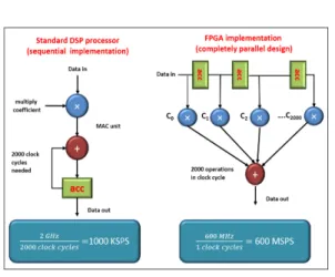
Fig. 2 shows the difference between a DSP
and FPGA based simple calculation and
illustrates how an FPGA computes faster than
Fig. 2 Difference between a DSP processor operation and FPGA based operation
even the DSP while implementing a simple tap filter that utilizes parallelism, compared with a sequential operation of a DSP.
Section 2 of this paper discusses the details of the UWPI algorithm. Section 3 discusses the implementation of the UWPI algorithm with the FPGA, along with details of implementation at the hardware level. It also describes the communication of the FPGA board with the computer and interfacing protocol. The final results are presented in section 4.
2. Ultrasonic Wave Propagation Imaging Algorithm
In a wave propagation imaging system, a three-dimensional (3D) data structure is used to generate the results, such as a video, to visually detect/evaluate the damage. In the post- processing technique, the results generation (video) process starts only when all the data (all the acquired ultrasonic signals) are completely saved after the scanning process is finished.
The UWPI algorithm is an example of such process that maps the acquired ultrasonic signal from the data acquisition (DAQ) system into a spatial-temporal data structure based on the three-dimensional (3D) data mapping algorithm.
The result of the 3D data mapping algorithm is
Fig. 3 3D data processing for conventional UWPI
UWPI.
Fig. 3 shows the block diagram for the software based conventional UWPI process. The process starts with an ultrasonic signal acquisition using the DAQ system and sampled at the signal length of samples with the sampling time interval of for every laser impinging raster scanning. The 3D data mapping function receives the signal and each sample in the ultrasonic signal is stored in spreadsheets.
The data points were then stored in the spreadsheet corresponding to its local laser impinging point. This process continues to map the samples of the ultrasonic signal into the created spreadsheets according to their respective laser impinging points as soon as the data is available in the buffer of the DAQ system. After all the signals are transferred for the entire area of interest, the 3D data structure, as shown in Fig. 3, is formed and ready for video generation [8]. A similar procedure is applied for the post processing system, with the data acquisition from DAQ card being replaced by the data transfer from the computer itself, using the already stored data.
3. FPGA Implementation of UWPI Algorithm
This section describes the details of the
UWPI algorithm implementation in FPGA and
how the FPGA based DSP board communicates
with the computer for video generation.
Fig. 5 FPGA based DSP board
Fig. 6 UWPI block diagram Fig. 4 Ultrasonic propagation imaging system with
a Q-switched laser, a laser mirror scanner, and an ultrasonic sensor
3.1. Overview of FPGA Based Wave Imaging Method in Ultrasonic Wave Propagation Imaging System
As shown in Fig. 4, the UPI system has a laser scanning system based on a Q-switched laser which excites energy in the specimen with laser pulses. The scanning was controlled via a laser mirror scanner (LMS). Both the Q-switched laser and LMS were controlled by an external computer. Fig. 4 shows the scanning system based on Q-switched laser and LMS.
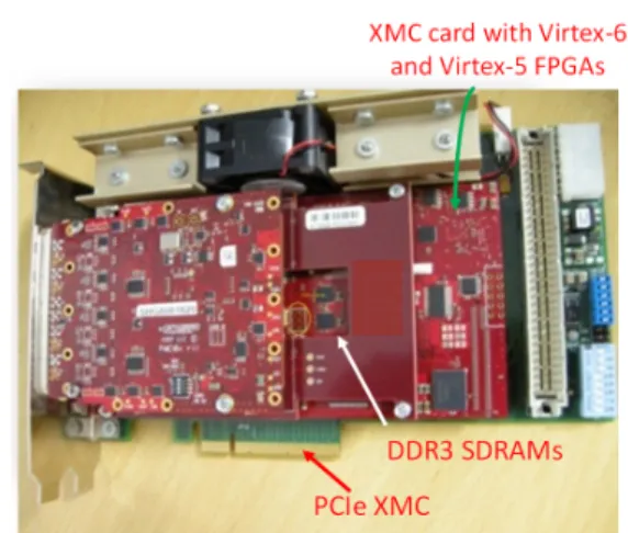
The DSP board includes FPGA Virtex-6 chip having high speed logic fabric with 30- million-gates which is the heart of the system for implementation of the image/signal processing algorithm. A secondary FPGA device is used for the peripheral component interconnect express (PCIe) communication. This FPGA communicates directly with the PCIe switched mezzanine card (XMC) card integrated with the board. It provides a transparent interface between the Virtex-6 device and the PCIe XMC card using 4 lanes (PCIe x4) communication [22].
The DDR3-SDRAM memory [20] is used as a data storage medium. A 4 Gbit DDR3-SDRAM (512 mega byte) high performance memory with 533 MHz frequency is used for this purpose.
The installed capacity is 2 gigabyte (GB) (four 512 megabyte (MB) memories), but for the test experiment one DDR3 of 512 MB is utilized.
For this purpose, an SDRAM controller is needed and hence the Xilinx SDRAM controller intellectual property (IP) core is utilized and programmed within the FPGA. Fig. 5 shows the actual hardware used for the system development.
3.2. Implementation and Working 3.2.1. Hardware and Firmware
With the conventional UWPI implementation,
the processing load is transformed to the
processor and the algorithm implementation is
performed with the software, which inherently
causes slower operations relative to any dedicated
system. In the FPGA based system, the imple-
mentation of the algorithm is at the hardware
level itself. This provides the benefit of data
processing at the binary/gate level without any
extra transformation, as is required for a
Fig. 7 RTL for the UWPI module
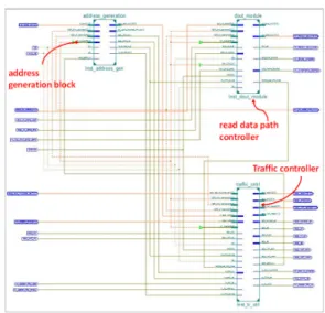
software based system, and also means that the data-processing is implemented over a dedicated area of hardware. Fig. 6 shows how the UWPI algorithm is implemented at the hardware level with FPGAs.
Three main sub-modules exist: the address generator, the traffic controller, and the read data path controller. The purpose of these sub-modules is as follows in respective order:
generate addresses for reading and writing processes, control the traffic relative to memory controller, and collect and accumulate data fetched from the DDR3-SDRAM memory.
The process starts with an ultrasonic signal (data) being stored in the buffer (called direct memory access (DMA) first in first out (FIFO) input buffer), and the corresponding address is then generated by the address generator (which also acts as an initiator block-initiating the UWPI process as it starts the generating address). Note that the DDR3 memory addresses are divided into ROWs, BANKS, and COLUMNs [20], but the memory controller IP provides a flat address space for the end user [21]. Hence, the counter mechanism was used for addressing the appropriate memory locations for the respective signals and samples.
The controller IP communication is divided into two main paths: (i) the address and command path and (ii) the data path. The traffic controller block is responsible for the address path (both for read and write cycle) and the write data path. The address generation block (see Fig. 6) generates the addresses and commands (writing or reading) and buffers them in a FIFO inside the traffic controller block. The traffic controller then fetches these commands and addresses, along with the respective data from DMA-in FIFO (for write data cycle), and passes them to the memory controller.
For the read data cycle, the address path design is the same, while the read data cycle is managed and organized by the read data path
controller. This block collects the data and saves it in the DMA out FIFO, which is then available for the PC to fetch through DMA transfer via the PCIe interface and to generate the video. Fig. 7 shows the register transfer level (RTL) diagram generated with the Xilinx synthesizer (XST). It presents the register level implementation of the design, describes the address generation, read data path controlling and traffic controlling operations performed on incoming data. It also specifies the controlling signals used at each operator to manage the transfer of data.
3.2.2. Software
The FPGA based DSP board needed to communicate with the computer through some communication protocol. Hence, an XMC card was used with the PCIe protocol. A visual C++
(VC++) based interface was developed using a visual studio compiler to control the communi- cation.
Two main communication channels exist: the
command channel and data channel. While the
command channel only performs tasks such as
sending commands to the FPGA internal
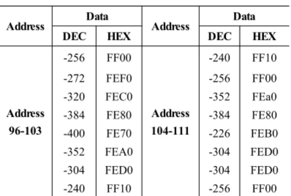
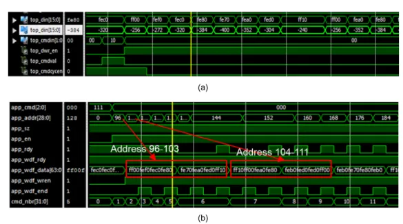
Table 1 Verification data for simulation
Address Data
Address Data
DEC HEX DEC HEX
Address 96-103
-256 FF00
Address 104-111
-240 FF10
-272 FEF0 -256 FF00
-320 FEC0 -352 FEa0
-384 FE80 -384 FE80
-400 FE70 -226 FEB0
-352 FEA0 -304 FED0
-304 FED0 -304 FED0
-240 FF10 -256 FF00
hardware and firmware section. However, the reading procedure from the board is somewhat complicated. Since the DMA transfer is extremely fast compared to the file-saving mechanism in the software, multi-threading was utilized to vitalize the DMA benefits while reading data from the DSP board. The idea involved using the virtual parallelization of the CPU with threading and dividing the load that is being consumed using the serialized processing and file saving while reading from the FPGA.
Fig. 8 shows how the multi-threading method in visual C++ was used to distribute the task of saving multiple files simultaneously. This way, the processor resources were shared to overcome the processor based operation bottleneck between the fast FPGA speeds and the slower CPU processing.
Fig. 8 Flow chart for multi-threading operation for file reading from DSP board
diagram shown in Fig. 9 presents the addresses generated using address generator and data stored in each address. The expected data in each address is shown in Table 1 for the verification of simulated result. Since, we are loading the data from the text file to the DDR3 memory therefore the sequence of the data is mentioned in Table 1 to match with the data in write data path of memory controller. It can be seen that for address 96-103 in Fig. 9(a), the data (in hex format) complies with the address shown in Table 1. The 16 bit data is concatenated to form 64 bit word for memory controller which takes two 64 bit words and store in 8 memory locations for address 96-103 and address 104-111 as shown in Fig. 9(b).
The final results were generated and
compared with the conventional CPU based
system (C#-LabVIEW based system). Fig. 10
shows the snapshots from videos generated from
the conventional system, as reference, and from
the FPGA based system. Ultrasonic waves
emerging from the sensor location propagating
(a)
(b)
Fig. 9 Simulation result for write data path using memory controller and DDR3 simulation model
Fig. 10 Imaging results for 200×200 mm2 scanning, (a) freeze frames from FPGA-based system, (b) freeze frames from C#-LabVIEW-based system
Fig. 11 Graph comparing performance of FPGA- based and CPU-based systems
![Fig. 1 UPI system performance comparison between 64-bit and 32-bit operating system [10]](https://thumb-ap.123doks.com/thumbv2/123dokinfo/4744256.514350/2.808.90.390.118.296/fig-upi-performance-comparison-bit-bit-operating.webp)