논문 2012-50-3-5
바이오응용 무선전력전달을 위한 13.56 MHz CMOS 다단 정류기
( A 13.56 MHz CMOS Multi-Stage Rectifier for Wireless Power Transfer in Biomedical Applications )
차 혁 규
* * ( Hyouk-Kyu Cha )
요 약
0.18-µm CMOS 반도체 공정을 이용하여 신체에 깊이 이식되어 있는 deep implant 의료 전자기기에서의 무선전력전달을 위 한 고효율의 다단 정류기 (multi-stage rectifier)를 구현하였다. 세 개의 단계로 이루어진 정류기는 cross-coupled 된 구조를 이용하여 외부에서 전달되는 작은 AC 입력 신호를 boost하여 1.2-1.5 V의 DC 출력 신호를 implant 전자기기로 전달한다. 설 계 된 정류기는 13.56 MHz에서 0.6-Vpp의 작은 RF 입력 신호와 10-kΩ의 load 저항이 연결 된 측정 환경에서 최대 70 %의 전력 변환 효율을 달성하였다.
Abstract
An efficient multi-stage rectifier for wireless power transfer in deep implant medical devices is implemented using 0.18-µm CMOS technology. The presented three-stage rectifier employs a cross-coupled topology to boost a small input AC signal from the external device to produce a 1.2-1.5 V output DC signal for the implant device. The designed rectifier achieves a maximum measured power conversion efficiency of 70% at 13.56 MHz under the conditions of a low 0.6-Vpp RF input signal with a 10-kΩ output load resistance.
Keywords
:CMOS rectifier, multi-stage rectifier, gate cross-coupled, wireless power transfer, biomedical implant devices
Ⅰ. Introduction
One of the most important issues in the development of implantable biomedical devices is the consistent provision of a stable and reliable power supply. Wireless inductive links are widely used for this purpose as batteries require a periodic replacement which causes much inconvenience and
*
정회원, 서울과학기술대학교 전기정보공학과
(Department of Electrical and Information Engineering, Seoul National University of Science and Technology)
※ 이 연구는 서울과학기술대학교 교내 학술연구비 지 원으로 수행되었습니다.
접수일자:2012년10월23일, 수정완료일:2013년2월15일
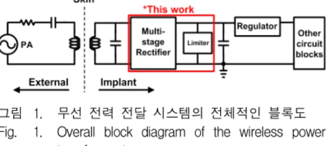
risk to the patient. The transfer efficiency is an important parameter for this wireless power link as the amount of transmitted power can be reduced and/or a longer distance link can be achieved. Deep implant medical devices such as blood flow sensor [1], which is placed deep inside the patient, especially require a highly efficient wireless power transfer system which achieves maximum efficiency and generate large enough output DC voltage at low AC input signal power. Fig. 1 shows the typical wireless power transfer system, consisting of the external power delivery part, inductive coils, rectifier, and a regulator. The overall efficiency of the transfer system can be represented as;
그림 1. 무선 전력 전달 시스템의 전체적인 블록도 Fig. 1. Overall block diagram of the wireless power
transfer system.
×
×
×
(1)
where
represents the power amplifier efficiency,
is the inductive coil link efficiency between the external and internal coils,
is the efficiency of the rectifier, and
represents the regulator efficiency. The efficiency of the rectifier is usually the key factor on the internal side in achieving high overall transfer efficiency since the coil efficiency is limited due to the physical constraints of the implant coil while high regulator efficiency can usually be achieved.In this paper, we present a CMOS rectifier for wireless power transfer in deep implant applications which uses three cascaded stages to achieve high efficiency at low input signal power and generate a large enough output DC voltage for the implant device. Section II discusses required specifications while Section III describes the conventional solutions and the designed circuit in detail. Section IV presents the experimental results followed by the conclusions in Section V.
Ⅱ. Specification
The target application for the presented rectifier is an implantable blood flow monitoring system which is to be embedded in a prosthetic graft for early graft failure detection[2]. Prosthetic vascular grafts are frequently applied in vascular surgery for bypass in lower limb ischemia or as a haemodialysis conduit in renal failure. Graft failure can result in deleterious consequences for the patients and therefore the measure of blood flow rates in these grafts can serve as a valuable prediction of subsequent thrombosis
그림 2. 무선 전력 전달 과정 Fig. 2. Power delivery chain.
and failure.
The implant device is to be embedded up to 50 mm deep inside the human body and therefore the wireless power transfer system has to provide a reliable power and supply voltage to the circuits inside the implant. The external device is to supply 200 mW to the implant device. Assuming an industrical, scientific, and medical (ISM) band frequency of 13.56 MHz is used, the tissue loss for 50 mm distance is approximately 25 dB[2].
As the in-body environment constraints the size and space available, the external and internal coupling coils are quite different. The external coil can be as large as 10 cm in diameter, while the internal coil can have up to 6 mm, which critically degrades the coupling efficiency to around 10%. As the implant device requires around 20 µW power for operation, the combined efficiency of the rectifier and the following low-dropout regulator (LDO) has to be over 45%.
Assuming the LDO can achieve 80% efficiency, the power conversion efficiency of the rectifier must meet over 60% for the system with some margin. This specification is illustrated in Fig. 2.
Due to the long distance and poor efficiency in the coils, the incoming AC input voltage to the following rectifier input can be as low as 600 mVp-p. As the internal circuit blocks of the monitoring system operate at a low supply voltage of 1-V, the following low-dropout regulator (LDO) after the rectifier in the wireless power transfer chain needs to receive over 1.2 V DC voltage as its input to produce 1 V DC to the rest of the circuit blocks, assuming the LDO efficiency is around 70 to 80%. To summarize the
(a)
(b)
그림 3. 기존의 정류기 회로도 (a) full-wave 다이오드 정류기 (b) 비교기 기반의 정류기
Fig. 3. Schematic of the conventional rectifiers.
(a) full-wave diode rectifier (b) comparator-based rectifier
requirements for the design, the rectifier has to be able to provide at least 1.2-V DC output from a 13.56 MHz input AC voltage signal of 600 mVp-p with an efficiency of over 60%.
Ⅲ. CMOS Rectifier Design
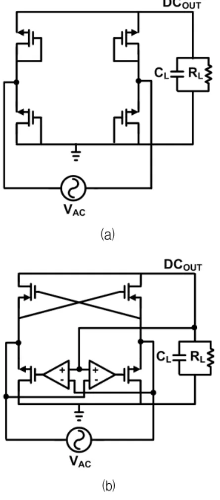
1. Conventional Rectifiers
There are several rectifiers which are widely used for wireless power transfer in both consumer and biomedical applications. The most typical topology is the full-wave diode-bridge rectifier shown in Fig.
3(a). This topology, however, has a limitation in achieving a high efficiency since it requires two threshold voltage drops across the diodes for operation[3]. Another popular rectifier type is the comparator-based rectifier shown in Fig. 3(b)[4∼9].
High efficiencies have been achieved through the usage of comparators in order to maximize the forward current while minimizing the reverse leakage current. The utilization of dynamically powered comparators allows low power consumption while achieving a highly efficient rectifier. The problem of these comparator-based rectifiers is that it requires a large enough input AC signal of over two threshold voltage drops in order for the comparator to start-up.
Without the comparator in operation, the rectifier shows a dramatic degradation in efficiency in low input signal region and thus is not appropriate for deep implant applications.
2. Proposed Rectifier Circuit Design
The rectified output DC voltage can be expressed as;
(2)
In order for the rectifier to operate at small input voltage while delivering the required output voltage and achieve high efficiency, the voltage drop has to be minimized. Also, multiple stages are needed so that the small input signal may be boosted to produce a sufficiently large output voltage. A gate cross-coupled circuit topology is employed for this purpose to realize the multi-stage rectifier for the implant system. The advantage of this rectifier is that it has a low on-resistance during operation which enables small voltage drop in comparison to the full-wave diode-bridge rectifier and the comparator-based types. Most importantly, the rectifier can operate at small input swings as low as down to around one threshold voltage due to its structure as shown in Fig. 4. The rectifier consists of NMOS and PMOS transistors operating as switches in which the gates are driven by the differential input RF signal.
In the positive cycle of the operation (when RF+ is high),
and
will turn on and the current will flow to the load consisting of
and
to produce the rectified DC voltage. At this cycle, both그림 4. 제안 된 CMOS 정류기의 회로도
Fig. 4. Schematic of the proposed CMOS rectifier.
그림 5. 세 단계 정류기의 블록도
Fig. 5. Block diagram of cascaded three-stage rectifier.
그림 6. 정류기 출력에 연결 된 DC limiter의 회로도 Fig. 6. Schematic of DC limiter at the rectifier output.
and
will be OFF. In the negative input cycle, the rectifier will operate similarly with
and
. The sizing of the transistors affects the on-resistance value and therefore is important in deciding the maximum efficiency of the rectifier. The power conversion efficiency (PCE) should be maximized in the minimum input condition so that the minimum amount of power that must be supplied to the implant device is guaranteed in the worst case scenario. With careful simulations considering the minimum input signal level and output load resistance which mimics the amount of current that must be0.5 1.0 1.5 2.0 2.5
0.2 0.4 0.6 0.8 1.0 1.2 1.4 1.6
O u tput DC V o lt age ( V )
Input AC Voltage (Vpp)
Typical SS FF
그림 7. 입력 AC 전압 대 출력 DC 전압에 대한 코너 시뮬레이션
Fig. 7. Corner simulation plot of increasing AC input voltage versus DC output voltage.
supplied to the whole internal device, the W/L sizing of the PMOS and NMOS transistors are decided to be 316µm/0.18µm and 68µm/0.18µm, respectively.
Active body biasing circuit, consisting of
and
transistors, are used to make sure the body nodes of
and
are always tied to the higher potential of RF input or DC output.As shown in Fig. 5, three stages of gate cross-coupled rectifiers are cascaded to boost the output voltage up to 1.2 V at 600 mVp-p input condition. Metal-insulator-metal (MIM) capacitors are used at the input of second and third stage rectifier inputs for charge storage for multi-stage boost operation. A DC limiter, shown in Fig. 6, is employed to limit the rectifier output DC voltage at 1.5 V so that the following circuit blocks are protected from the resulting high voltage signal assuming the distance between the external and internal devices get too close to each other. Diode-connected low-threshold PMOS devices are used to realize the limiter.
Fig. 7 shows the process corner simulation results of the input AC signal versus output DC voltage for the designed three-stage rectifier. The simulation is carried out at 13.56 MHz input frequency and at 37.5°C temperature to mimic in-body temperature with a load of 10-kΩ resistor and 10-µF capacitor.
The results show that at least 1.2 V is achieved at
0.5 0.6 0.7 0.8 0.9 1.0 1.1 10
20 30 40 50 60 70 80 90
PCE Vout
Input AC Voltage (Vpp)
Eff ic ien cy ( % )
0.6 0.8 1.0 1.2 1.4 1.6 1.8 2.0 2.2 2.4 Ou tp ut DC Volt ag e (V)
그림 8. 입력 AC 전압 대 변환 효율 및 출력 DC 전압 에 대한 시뮬레이션
(출력 단에 DC limiter는 불포함)
Fig. 8. Simulation plot of varying AC input voltage versus effciency and output DC voltage.
(DC limiter removed at the output)
그림 9. 정류기의 칩 사진
Fig. 9. Chip microphotograph of three-stage rectifier.
all process corners with the specified minimum input voltage at 600 mVp-p. Also, the limiter is able to limit the output DC voltage below 1.6 V at different corners. Fig. 8 presents the varying input versus PCE and output DC voltage simulation results under the same condition as the previous simulation. The output DC limiter is disconnected in this simulation.
A maximum simulated PCE of 76% is achieved around the low input AC voltage of 590 to 650 mVp-p. A steep increase in the output DC voltage and PCE in the 500 to 600 mVp-p input voltage region is due to the start-up of rectifier transistors for operation.
Ⅳ. Experimental Results
The designed rectifier is fabricated in a one-poly six-metal (1P 6M) 0.18-µm CMOS process. The chip
0.5 0.6 0.7 0.8 0.9 1.0
0.6 0.8 1.0 1.2 1.4 1.6
Output DC V o lt age ( V )
Input AC Voltage (Vpp)
그림 10. 입력 AC 전압 대 출력 DC 전압의 측정 결과 Fig. 10. Measured output DC voltage versus varying
input AC voltage.
그림 11. 입력 AC 전압 대 변환 효율의 측정 결과 Fig. 11. Measured PCE versus varying input AC voltage.
microphotograph is shown in Fig. 9, where the area of the core is 0.125 mm². Most of the layout area is consumed by the MIM interstage input capacitors of the second and third stage rectifier. Much attention is given in the input layout path as parasitic resistance degrades the efficiency. The die is housed in a quad flat nonleaded (QFN16) package for measurement on a FR4 PCB. The default measurements are done at 13.56-MHz input frequency with an output load of 10-kΩ resistor and 10-µF capacitor.
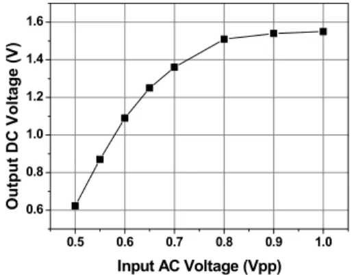
The measured rectified output DC voltage versus varying input AC voltage is shown in Fig. 10. The output DC voltage increases linearly to the input signal until it reaches 1.55 V which is limited by the output limiter circuit.
In order to measure the PCE, which is defined as;
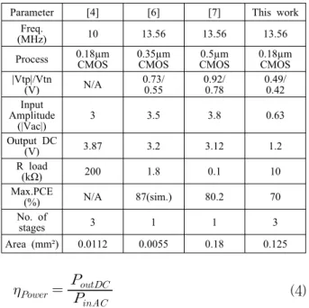
Parameter [4] [6] [7] This work Freq.
(MHz) 10 13.56 13.56 13.56
Process 0.18µm
CMOS 0.35µm
CMOS 0.5µm
CMOS 0.18µm CMOS
|Vtp|/Vtn
(V) N/A 0.73/
0.55 0.92/
0.78 0.49/
0.42 Input
Amplitude
(|Vac|) 3 3.5 3.8 0.63
Output DC
(V) 3.87 3.2 3.12 1.2
R load
(kΩ) 200 1.8 0.1 10
Max.PCE
(%) N/A 87(sim.) 80.2 70
No. of
stages 3 1 1 3
Area (mm²) 0.0112 0.0055 0.18 0.125
표 1. 저주파 CMOS 정류기들의 비교 테이블 Table 1. Low-frequency CMOS Rectifier Benchmark for
Wireless Power Transfer Applications.
(4)
both the input and output power has to be measured and offline calculate the resulting PCE. To measure the input power, the input current is calculated by placing a small series resistor at the input of therectifier on the PCB and the voltage between the resistor terminals is measured. A maximum PCE of 70% is measured at an input voltage of 650 mV, as shown in Fig. 11.
Table I compares the presented three-stage rectifier with previous low-frequency CMOS rectifiers. Although higher efficiency is achieved in the previous rectifiers using comparators for switching control, a large input signal is required for operation. With regards to the small input signal required for operation, the implemented rectifier compares favorably to the previous works while still achieving a good conversion efficiency and satisfying the required specifications.
V. Conclusions
A highly efficient multi-stage rectifier for deep implant applications is implemented using 0.18µm CMOS process. A cross-coupled topology is utilized to facilitate low-input operation, while three cascaded
stages are used to produce a large DC output for the following stages in the implant device. A power conversion efficiency of 70% is achieved at 13.56 MHz under conditions of a 600-mVpp RF input signal with a 10-kΩ output load resistance.
References
[1] P.B. Khannur, K.L. Chan, J.H. Cheong, K. Kang, A.A. Lee, X. Liu, H.J. Lim, K. Ramakrishna, and M. Je, “A 21.6uW inductively powered implantable IC for blood flow measurement,” in
IEEE Asian Solid-State Circuits Conf., Nov.
2010
[2] R.-F. Xue, J.H. Cheong, H.-K. Cha, X. Liu, P.
Li, H.J. Lim, L.S. Lim, M.-Y. Cheng, C. He, W.-T. Park, and M. Je, “Ultra-low-power wireless implanable blood flow sensing microsystem for vascular graft applications,” in
IEEE Intl. Symp. Integ. Circuits, Nov. 2011
[3] C.-L. Chen, K.-H. Chen, and S.-I. Liu,“Efficiency-enhanced CMOS rectifier for wireless telemetry,” Electronic Letters, vol.43, no.18, Aug.
2007
[4] S.T. Kim, T. Song, J. Choi, F. Bien, K. Lim, and J. Laskar, “Semi-active high-efficient CMOS rectifier for wireless power transmission,” in
IEEE RF Integrated Circuits Symposium, Jun.
2010, pp. 97-100
[5] S. Guo and H. Lee, “An efficiency-enhanced CMOS rectifier with unbalanced-biased comparators for transcutaneous-powered high-current implants,” IEEE J. of Solid-State
Circuits, vol.44, no.6, pp. 1796-1804, Jun. 2009
[6] Y.-H. Lam, W.-H. Ki, and C.-Y. Tsui,“Integrated low-loss CMOS active rectifier for wirelessly powered devices,”
IEEE Trans.
Circuits and Systems II, vol. 54, no. 6, pp.
1378-1382, Jun. 2006
[7] H.-M. Lee and M. Ghovanloo, “An integrated power-efficient active rectifier with offset-controlled high speed comparators for inductively powered implants,” IEEE Trans.
Circuits and Systems I, vol. 58, no. 8, pp.
1749-1760, Aug. 2011
[8] 최영수, 부영건, 박준성, 임승옥, 문연국, 김선희, 이강윤, “CMOS 공정을 이용한 고효율 Active Rectifier 설계,” 대한전자공학회 2011년 SoC학술 대회, pp.262-265, Apr., 2011
[9] 최영수, 이강윤, “넓은 입력 범위를 갖는 무선 전
저 자 소 개 차 혁 규(정회원)
2003년 KAIST 전기및전자공학과 학사 졸업.
2009년 KAIST 전기및전자공학과 박사 졸업.
2009년∼2012년 Institute of Microelectronics, Singapore, Senior Research Engineer 2012년∼현재 서울과학기술대학교
전기정보공학과 조교수
<주관심분야 : CMOS RF/Analog IC design for wireless communications and biomedical applications>
력 전송용 다중 모드 정류기 설계,” 대한전자공학
회, 전자공학회논문지-SD, 제49권 SD편, 제4호, pp. 34-42, Apr. 2012.