Vol. 27, No. 7 (2017)
364
Improving Interface Characteristics of Al
2O
3-Based Metal-Insulator-Semiconductor(MIS) Diodes Using H
2O
Prepulse Treatment by Atomic Layer Deposition
Hogyoung Kim
1†, Min Soo Kim
2, Sung Yeon Ryu
2and Byung Joon Choi
21Department of Visual Optics, Seoul National University of Science and Technology, Seoul 01811, Republic of Korea
2Department of Materials Science and Engineering, Seoul National University of Science and Technology, Seoul 01811, Republic of Korea
(Received May 18, 2017 : Revised Jun 7, 2017 : Accepted Jun 9, 2017)
Abstract
We performed temperature dependent current-voltage (I-V) measurements to characterize the electrical properties of Au/Al2O3/n-Ge metal-insulator-semiconductor (MIS) diodes prepared with and without H2O prepulse treatment by atomic layer deposition (ALD). By considering the thickness of the Al2O3 interlayer, the barrier height for the treated sample was found to be 0.61 eV, similar to those of Au/n-Ge Schottky diodes. The thermionic emission (TE) model with barrier inhomogeneity explained the final state of the treated sample well. Compared to the untreated sample, the treated sample was found to have improved diode characteristics for both forward and reverse bias conditions. These results were associated with the reduction of charge trapping and interface states near the Ge/Al2O3 interface.Key words
H2O prepulse treatment, atomic layer deposition(ALD), Al2O3 interlayer.1. Introduction
The modulation of Schottky barrier height(SBH) has been demonstrated by inserting a thin dielectric layer such as Al
2O
3,
1,2)Ge
3N
4,
3)GeO
x,
4)MgO,
5)Si
3N
4,
6)and TiO
27)between the metal and Ge contacts. When the thin inter- facial layer is present, the Fermi level of the metal is released toward the conduction band of Ge, alleviating the Fermi level pinning(FLP) effect and yielding a lower SBH. As a possible mechanism, it was proposed that the inserted insulating layer can block the electron wave function from metal to semiconductor and therefore de- crease the number of metal induced gap states(MIGS).
8)The dipole formed at the metal/semiconductor(MS) inter- face has been proposed to cause the potential drop to modulate the SBH.
9)It was also proposed that the fixed charges in the non-ideal dielectric layers would cause an extra potential drop across the dielectric layer.
10)As a method to deposit such interfacial layers, atomic layer deposition(ALD) can be used to obtain high-quality di- electric layer due to the accurate thickness control and
reproducibility.
Lee et al. investigated the electronic passivation of a Ge (100) surface, via the chemisorption of H
2O at room temperature(RT) using scanning tunneling microscopy (STM) and scanning tunneling spectroscopy(STS) and found that a majority of the surface is covered by H
2O chemisorbed dimer ( −OH and −H terminations of the dangling bonds on the dimer), single and double dangling bond sites.
11)The H
2O chemisorption can passivate the Ge surface by terminating dangling bonds. However, the coverage of H
2O is limited at elevated temperature. As suggested by Papagno et al., the H
2O adsorption on Ge (100) can be enhanced when the sample is cooled down at liquid nitrogen temperature.
12)The density functional theory(DFT) calculations showed that the reaction of trimethylaluminum(TMA) is more favorable on the Ge- OH sites than on the Ge-H sites, although both reactions are favorable from a thermodynamic point of view.
13)In either case, H
2O prepulsing in ALD process can enhance the possibility to form thermally stable Ge-O-Al bonds.
Using in-situ H
2O prepulsing on the bottom electrode
†Corresponding author
E-Mail : [email protected] (H. Kim, Seoul Nat'l Univ. Sci. Thch.)
©Materials Research Society of Korea, All rights reserved.
This is an Open-Access article distributed under the terms of the Creative Commons Attribution Non-Commercial License (http://creative- commons.org/licenses/by-nc/3.0) which permits unrestricted non-commercial use, distribution, and reproduction in any medium, provided the original work is properly cited.
prior to ALD, Lin et al. showed that the electrical per- formance of high-k metal-insulator-metal(MIM) capacitors can be improved.
14)Swaminathan et al. reported that H
2O prepulsing can be used to prepare less defective Ge metal-oxide-semiconductor(MOS) devices with ALD-Al
2O
3as a gate insulator.
15)In Au/Al
2O
3/InP metal-insulator- semiconductor(MIS) Schottky structures, the increased SBH was observed when the Al
2O
3thickness is larger than 5 nm.
16)SBH larger than the Ge band gap has been observed, which was explained through the formation of an inversion layer at the NiGe/n-Ge interface.
17)This observation was regarded to be technologically important because NiGe is an ideal Schottky source/drain material in Ge-based p-MOSFETs due to the absence of energy barrier between NiGe and p-Ge. Liu et al. demonstrated that when the thickness of amorphous-Ge reaches above 10 nm, the Al/amorphous-Ge/n-Ge shows ohmic charac- teristics, associated with electron hopping through localized states of amorphous-Ge layer as well as the termination of dangling bonds at the amorphous-Ge/n-Ge interface.
18)Hence, it will be meaningful to investigate the physical properties governing the metal/n-Ge diodes with an Al
2O
3interlayer (thickness greater than 10 nm). Here, we com- paratively investigated the electrical properties of Au/
Al
2O
3/n-Ge MIS diodes with and without H
2O prepulse treatment prepared by ALD.
2. Experimental
Sb-doped Ge (100) wafer (thickness: 500 μm, carrier concentration: 5 × 10
15cm
−3) grown by Czochralski method, was used in this investigation. The wafer was cut into small pieces (about 5 × 10 mm
2) and were loaded into an ALD chamber within a minute of the cleaning process to minimize exposure to air. Then, the deposition temperature ramped up to 250
oC for 5 min in an N
2ambient (200 SCCM and 100 mTorr). Before deposition, some of the pieces were subjected to H
2O prepulse treatment for 3 min. Then Al
2O
3thin film was deposited at 250
oC.
TMA and deionized water were used as the precursors with a purging gas of nitrogen (N
2). Pulse sequence was composed of TMA (1s), N
2purge (5s), H
2O (0.5s) and N
2purge (25s). Using spectroscopic ellipsometer, the Al
2O
3thickness was measured to be about 15 nm. After solvent cleaning, gold(Au) Schottky contacts with thick- nesses of 50 nm were deposited by using radio-frequency (RF) magnetron sputtering through a shadow mask onto the Al
2O
3layer of all the samples. For ohmic contacts, Al metal with a thickness of 150 nm was deposited and then In metal was rubbed over the entire back surface of the samples. Current-voltage ( I-V) and capacitance-voltage ( C-V) measurements were carried out with a Keithley 238 current source and an HP 4284A LCR meter. I-V
measurements under various temperatures were performed using a hot chuck connected with a temperature controller.
3. Results and Discussion
The forward bias I-V characteristics measured at room temperature were analyzed based on the TE model.
19)The effective barrier heights ( φ
B) were determined to be 0.71 (± 0.06) and 0.70 (± 0.03) eV, for the samples with and without H
2O prepulse treatment, respectively. The ideality factors were calculated to be 1.50 (± 0.19) and 1.93 (± 0.20), for the samples with and without H
2O prepulse treatment, respectively. Note that the barrier height and the ideality factor for the Au/n-Ge Schottky diodes (i.e., without Al
2O
3interlayer) measured at room temperature were found to be 0.59 (± 0.03) eV and 1.54 (± 0.23), respectively. This indicates that the insertion of Al
2O
3interlayer mainly enhanced the barrier height. Fig.
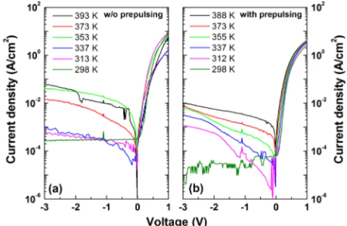
1 shows the typical semi-logarithmic I-V plots for both samples measured at different temperatures, which reveal rectifying characteristics over the entire temperature range.
For the sample with H
2O prepulse treatment, the current values increase monotonically with increasing the tem- perature. In contrast, the current values do not increase monotonically for both the forward and reverse bias con- ditions for untreated sample. Similar results were observed in Au/ZnO Schottky diodes,
20)which was associated with the fact that the surface compensation around the contact periphery due to acceptor-like adsorbates occurred to varying extents at each temperature.
21)In this work, the configuration of Au/Al
2O
3contact periphery (i.e., circles of a diameter of 300 μm) is the same for both samples.
Hence, the compensation due to acceptor-like defects, if present, may occur near the Al
2O
3/Ge interface. The inter- section of I-V curves under forward bias was attributed to the interfacial layer near the interface and the interface
Fig. 1. Semilogarithmic current-voltage (I-V) characteristics for the Au/n-Ge Schottky diodes (a) without and (b) with H2O prepulse treatment.
states and the effect of series resistance.
22,23)These I-V behaviors in Fig. 1 indicate that the diode characteristics were improved after H
2O prepulse treatment due to the suppression of interface defects at Al
2O
3/Ge interface.
The TE model was applied again to the forward bias I- V data in Fig. 1 to determine the barrier heights and the results of which are presented in Fig. 2(a). The increase of barrier height with increasing temperature was attributed to an inhomogeneous Schottky barrier.
24)The relation between barrier height and temperature can be described
as , where is a zero-bias mean
barrier height and σ
0is a standard deviation. The σ
0value for the sample with prepulse treatment (0.104 V) was smaller than that for the sample without prepulse treatment (0.189 V), indicating modification of the local barrier height.
With the lateral barrier inhomogeneity, the modified Richardson plot can be given by
(1) where I
0is the reverse bias saturation current, A is the contact area and A
**is the Richardson constant. Fig. 2(b)
shows plots of vs. 1/ kT. The
intercepts at the ordinate produced modified Richardson constants of 125.1 and 344.5 Acm
−2K
−2, respectively, for the samples with and without H
2O prepulse treatment.
The value for the treated sample is comparable to the theoretical value of 140.0 Acm
−2K
−2for n-type Ge, which implies that the TE model along with the barrier inhomo- geneity can explain the current transport properties of the Au/Al
2O
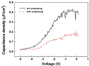
3/n-Ge MIS diodes. As shown in Fig. 3, the C-V curves measured at 500 kHz reveals that the capacitance values for treated sample are lower than that for treated sample. This can be due to the reduced contribution of interface states to total capacitance for the treated sample.
In addition, the flat band voltage( V
FB) of prepulse treated
sample seems to shift positively compared to that of untreated sample, associated with the compensation of positive charges in the oxide.
25)Meanwhile, the dielectric constants of Al
2O
3and GeO
2are known as 8-9
26)and 6.0,
27)respectively. During the H
2O prepulse treatment, Ge dangling bonds can be passivated, forming GeO
2layer.
Hence, Al
2O
3layer is grown on this GeO
2layer. When the very thin GeO
2layer is present between Al
2O
3and Ge layers, the average dielectric constant is lowered compared to the case of pure Al
2O
3layer. This will reduce the measured capacitance values. However, further in- vestigation is required to clarify the exact mechanism.
Still now, the thickness of Al
2O
3interlayer was not considered for the analysis. Considering the interfacial layer, the forward bias current density-voltage ( J-V) characteristics for the MIS Schottky diodes can be de- scribed as follows
19)J = A
**T
2exp( − δ)exp(−qφ
B/ kT)[exp(qV/nkT) − 1] (2) where n is the ideality factor, ζ (in eV) and δ (in Å) are the effective barrier and effective thickness of the inter- facial layer, respectively. For values of V greater than 3 kT/q, Eq. (2) can be expressed as
J ≈ A
**T
2exp( − δ) exp[−q/kT(φ
B− V/n)] (3) As shown in Fig. 4(a) for the treated sample, with plotting ln( J/T
2) vs. 1/ kT (Richardson plot) at different forward biases, a set of different E
avalues ( E
a= φ
B− V/
n) can be obtained from the slopes of the Richardson plots. Then, the barrier height can be determined from the linear fitting to the E
avs. V
Fplot shown in Fig. 4(b), which resulted in 0.61 eV. This value is similar to the barrier heights of 0.59 eV for the Au/n-Ge Schottky
φB = φB–qσ02⁄2kT φBI0⁄T2
( )
ln –q2σ02⁄2k2T2 = ln(AA**)–qφB⁄kT
I0⁄T2
( )
ln –q2σ02⁄2k2T2
ζ
ζ Fig. 2. (a) Barrier height vs. temperature and (b) modified Richardson
plot of ln(I0⁄T2)–q2σ02⁄2k2T2 vs. 1/kT.
Fig. 3. Capacitance-voltage (C-V) characteristics for both samples measured at 500 kHz.
diodes from the I-V data. The results indicate that we can enhance the barrier height from ~0.6 to ~0.7 eV by adding an Al
2O
3interlayer. Note that this method was not applied to the untreated sample because the current values do not vary monotonically as shown in Fig. 1(a).
Because the barrier height was about 0.71 eV with con- sidering the Al
2O
3interlayer(effective barrier height), the effective energy barrier across the Al
2O
3interlayer can be obtained using Eq. (2), which is given as ζ = . This effective barrier at room temperature was calculated to be about 0.07 eV.
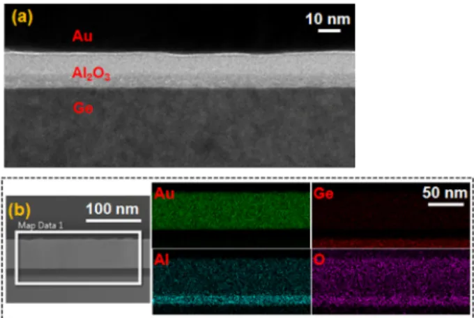
Fig. 5(a) shows the cross-sectional scanning transmission electron microscope(STEM) image around the Al
2O
3interlayer region for the treated sample, indicating that the Al
2O
3interlayer was grown uniformly on Ge surface.
The thickness of Al
2O
3measured by TEM is approxi- mately 15 nm. In order to investigate the distribution of each component near the Al
2O
3/Ge interface, energy-
dispersive X-ray spectroscopy(EDS) mapping was con- ducted for the elements of Au, Al, O and Ge. From the EDS mapping images shown in Fig. 5(b), Al
2O
3interlayer prepared with H
2O prepulse treatment shows that diffu- sion of Ge and Au atoms into the Al
2O
3interlayer is insignificant.
It was shown that the leakage characteristic of the near-stoichiometric Al
2O
3film is better than that of the oxygen-deficient one.
25)The dominant bonding state on the H
2O prepulsed Ge (100) prior to TMA exposure was found to be Ge-OH and this Ge-OH interfacial bonding is regarded to be beneficial in the reduction of charge trapping and fast interface state density, which eventually enhanced the concentration of adsorbed Al and thermally stable Ge-O-Al bonds serving as an ALD nucleation layer on Ge (100) surface.
15)Consequently, the oxygen- deficient Al
2O
3before H
2O prepulse treatment was trans- formed into near-stoichiometric Al
2O
3and the quality of the Al
2O
3film was improved after H
2O prepulse treatment.
4. Conclusion
Using current-voltage ( I-V) measurements, the tempera- ture dependent electrical properties of Au/Al
2O
3/n-Ge MIS diodes prepared with and without H
2O prepulse treatment by ALD were investigated. Compared to the untreated sample, the treated sample was found to have improved diode characteristics for both forward and reverse bias conditions. This was associated with the reduction of charge trapping and interface states near the Ge/Al
2O
3interface. Even though the thickness of Al
2O
3interlayer was 15 nm, the TE model with barrier inhomo- geneity explained well for the treated sample. Considering the thickness effect of Al
2O
3interlayer, the barrier height was found to be 0.61 eV, similar to those from the Au/n- Ge Schottky diodes. The result suggests that MIS diodes with improved performances were obtained using H
2O prepulse treatment.
Acknowledgments
This study was supported by the Research Program funded by the Seoul National University of Science and Technology (Seoultech).
References
1. Y. Zhou, M. Ogawa, M. Bao, W. Han, R. Kawakami and K. Wang, Appl. Phys. Lett., 94, 242104 (2009).
2. B. Coss, C. Smith, W. Loh, P. Majhi, R. Wallace, J. Kim and R. Jammy, IEEE Electron Device Lett., 32, 862 (2011).
3. R. Lieten, S. Degroote, M. Kuijk and G. Borghs, Appl.
φBeff–φB
( ) δ kT⁄( × ⁄q)
[ ]2
Fig. 4. (a) Richardson plot of the H2O prepusle treated sample under different forward biases and (b) plot of the activation energy (Ea) vs. the corresponding forward biases.
Fig. 5. (a) Cross-sectional scanning transmission electron micro- scope (STEM) image across the Al2O3 interlayer and (b) energy- dispersive X-ray spectroscopy (EDS) color mappings for each element scanned over the Au/Al2O3/Ge full structure.
Phys. Lett., 92, 022106 (2008).
4. T. Nishimura, K. Kita and A. Toriumi, Appl. Phys. Exp., 1, 051406 (2008).
5. D. Lee, S. Raghunathan, R. Wilson, D. Nikonov, K.
Saraswat and S. Wang, Appl. Phys. Lett., 96, 052514 (2010).
6. M. Kobayashi, A. Kinoshita, K. Saraswat, H. Wong and Y. Nishi, J. Appl. Phys., 105, 023702 (2009).
7. B. Tsui and M. Kao, Appl. Phys. Lett., 103, 032104 (2013).
8. T. Nishimura, K. Kita and A. Toriumi, Appl. Phys. Lett., 91, 123123 (2007).
9. J. Wager and J. Robertson, J. Appl. Phys., 109, 094501 (2011).
10. J. Hu, A. Nainani, Y. Sun, K. Saraswat and H. Wong, Appl. Phys. Lett., 99, 252104 (2011).
11. J. Lee, T. Kaufman-Osborn, W. Melitz, S. Lee and A.
Kumme, Surf. Sci., 605, 1583 (2011).
12. L. Papagno, D. Frankel, Y. Chen, L. Caputi, J. Anderson and G. Lapeyre, Surf. Sci., 248, 343 (1991).
13. J. Lee, T. Kaufman-Osborn, W. Melitz, S. Lee, A.
Delabie, S. Sioncke, M. Caymax, G. Pourtois and A.
Kummel, J. Chem. Phys., 135, 054705 (2011).
14. C. Lin, Y. Chen, C. Lee, H. Chang, W. Chang, H. Chang and C. Liu, J. Electrochem. Soc., 158, H128 (2011).
15. S. Swaminathan, Y. Oshima, M. Kelly and P. McIntyre, Appl. Phys. Lett., 95, 032907 (2009).
16. S. Zheng, W. Yang, Q. Sun, L. Chen, P. Zhou, P. Wang, D. Zhang and F. Xiao, Appl. Phys. Lett., 103, 261602 (2013).
17. D. Chi, R. Lee, S. Chua, S. Lee, S. Ashok and D. Kwong, J. Appl. Phys., 97, 113706 (2005).
18. H. Liu, P. Wang, D. Qi, X. Li, X. Han, C. Wang, S.
Chen, C. Li and W. Huang, Appl. Phys. Lett., 105, 192103 (2014).
19. S. Sze, Physics of Semiconductor Devices, Wiley, New York, (1981).
20. H. Von Wenckstern, S. Muller, G. Giehne, H. Hochmuth, M. Lorenz and, M. Grundmann, J. Electron. Mater., 39, 559 (2010).
21. H. Kim, A. Sohn and D. Kim, Semicond. Sci. Technol., 27, 035010 (2012).
22. O. Pakma, N. Serin, T. Serin and . Altlndal, Semicond.
Sci. Technol., 23, 105014 (2008).
23. J. Osvald and Zs. J. Horvath, Appl. Surf. Sci., 234, 349 (2004).
24. R. Tung, Mater. Sci. Eng., R 35, 1 (2001).
25. R. Garg, D. Misra and P. Swain, J. Electrochem. Soc., 153, F29 (2006).
26. J. Robertson and R. Wallace, Mater. Sci. Eng., R 88, 1 (2015).
27. J. Gu, Y. Liu, M. Xu, G. Celler, R. Gordon and P. Ye, Appl. Phys. Lett., 97, 012106 (2010).
Sç