Nanocommunication Design in Graduate-Level Education and Research Training
Tadashi Itoha,b*, Hisazumi Akaia,c, Seiji Takedaa,d, Hisahito Ogawaa, Satoshi Ichikawaa, Masaaki Geshia, Masato Araa, and Hirohiko Niiokaa
aThe Institute for NanoScience Design, Osaka University, Toyonaka, Osaka 560-8531
bDepartment of Materials Engineering Science, Osaka University, Toyonaka, Osaka 560-8531
cDepartment of Physics, Osaka University, Toyonaka, Osaka 560-0043
dThe Institute of Scientific and Industrial Research, Osaka University, Mihogaoka 8-1, Ibaraki, Osaka 567-0047
(Received July 1, 2010, Revised October 8, 2010, Accepted October 11, 2010)
In order to teach the accumulated knowledge of nanoscience, nanoengineering and nanotechnology to graduate school students and young scientists with the sense of public engagement, Osaka University started from 2004 to prepare and offer various kinds of education and training programs such as trans-disciplinary graduate-school minor program, evening course refresher program, short-term international research training program, etc. It offers a series of lectures, partly broadcasted live to satellite classrooms. In addition, the students can join intensive hands-on training programs using modern facilities, allowing them to design, fabricate, measure, characterize and functionalize nanomaterials and nanodevices. In addition, there are four specially designed lectures and research training programs aimed for nanocommunication including social, legal and ethical relationship: “Nanotechnology Career-up Lectures”, “Social Engagement on Nanotechnology”, “Road Map Design on Nanotechnology”, and “Project- Aimed Learning and Training Programs (PAL)”. The outline of the whole programs is described together with the specialized programs for nanocommunication.
Keywords : Nanoscience, Nanoengineering, Nanotechnology, Graduate-level education, Research training, Public engagement, Nano-communication
I. Introduction
The emerging fields of nanotechnology are leading to a technological innovation in the 21st century. The application of nanotechnology has enormous potential to greatly influence the scientific and engineering world in which we live. Advances in nanotechnology promise to have major implications for health, wealth, and peace in the upcoming decades. Knowledge in this field is lead-
ing to fundamental scientific and engineering advances.
In turn, this will lead to dramatic changes in the ways that materials, devices, and systems are understood and created. Research and development in nanotechnology is likely to change the traditional practices of design, analysis, measurement, and manufacturing for a wide range of engineering products.
Many scientists all over the world now realize the importance of education and research training in the
fields of nanoscience and nanoengineering, since they are really multi-/trans-disciplinary and become im- portant key technology for the sustainable develop- ment of many kinds of emerging fields. This impact creates a challenge for the academic community to ed- ucate a variety of students (not only in the fields of physics, chemistry, materials science, electronics and mechanics, but also in other fields such as bioscience, medicine, and even social science and humanity for public engagement, standardization and road map de- sign) with the necessary knowledge, understanding, and skills to interact and to provide leadership in the emerging world of nanotechnology. Osaka University established the Organization for the Promotion of Research on Nanoscience and Nanotechnology (OU- OPRNN) in April 2002, under the auspices of the Osaka University Research Promotion Office and started the careful planning of education and research training programs for two years. As a result, in order to hand on the accumulated knowledge of the related fields to graduate school students and young scientists who will design and develop new kinds of fields for fu- ture nanoscience, nanoengineering and nanotechnology together with the development of the public engage- ment, OU-OPRNN has started from 2004 to prepare various kinds of education and training programs such as trans-disciplinary graduate-level minor program, evening course refresher program, short-term inter- national research training program, etc. It offers a series of lectures, some of them in the form of dis- tance education broadcast live to satellite classrooms located at many places in Japan, and tentatively even overseas in English. In addition, the students can join intensive hands-on training programs using modern facilities equipped in and outside of the Institute, al- lowing them to design, fabricate, measure, character- ize and functionalize nanomaterials and nanodevices.
There are four specially designed lectures and re- search training programs for nanocommunication in- cluding social, legal and ethical relationship; (1) “Nano-
technology Career-up Lectures” (started in 2006) which are series of omnibus lectures taught by researchers and engineers working in nano-related industries and institutions by introducing various kinds of their knowl- edge and experiences. (2) “Social Engagement on Nanotechnology” (started from the spring semester of 2010) which is specialized in public engagement, risk assessment and management, standardization, etc. (3)
“Road Map Design on Nanotechnology” (beginning from the autumn semester of 2010) which introduces several important future industrial products together with their road maps, necessary appliance and public engagement of many kinds of basic elemental science and technology which may have relationship with the specialty of gradu- ate-level students. (4) “Project- Aimed Learning and Training Programs (PAL)” (started in 2005) which are offered by introducing several research subjects pro- posed by industries, each of which is co-supervised by university and industry research staffs and solved by a group of students, mainly PhD students, coming from different fields.
These programs are called as the Nanoscience-/
Nanotechnology-Related Advanced Inter-/Trans-/
Multi-Disciplinary Education Program and Refresher/
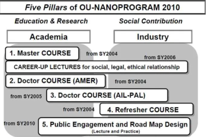
Training Courses offered by Osaka University, here- after referred to as OU-NANOPROGRAM and have been conducted by OU-OPRNN for four years and in 2008 the Institute for NanoScience Design was newly established and guarantees the long term offer of the OU-NANOPROGRAM. The Institute for Nanoscience Design accepts the part-time aid of the joint groups of lecturers and researchers belonging to six different graduate schools and six different research in- stitutions and centers related to nanoscience and nanoengineering and also in collaboration with the Osaka University Academia-Industry Liaison Consortium for Human Resource Development on Nano Science and Engineering (ALICE-ONE) by covering the liaison fields among social, human and natural sciences. The five pillars and the outline of OU-OPRNN are sum-
Figure 1. Structure of OU-NANOPROGRAM with academia- industry liaison consortium.
Figure 2. Outline of OU-NANOPROGRAM.
marized in Figs. 1, 2, respectively.
OU-NANOPROGRAM
Nanoscience, nanoengineering and nanotechnology are all open fields, which cannot be fitted within the boundaries of conventional scientific disciplines.
Therefore, the resulting curriculum should be multi-/
inter-/trans-disciplinary in nature, and it should be rapidly adaptable to newly emergent research fields.
It should be emphasized that systematic, fundamental research is a prerequisite to developing future science
and technology. Thus, instead of starting out with a completely new curriculum, it is rather natural to build a combined curriculum based upon the subjects currently being offered as major subjects in various major fields, and design the OU-NANOPROGRAM as a complementary minor program by keeping a proper balance between the major and minor programs.
The OU-NANOPROGRAM has been designed for the purpose of educating natural science and engineering students with the necessary knowledge, under- standing, and skills to interact and provide leader- ship in the nano-fields. The educational goals are to provide the students with the abilities for:
∙Design, analysis, and simulation of nano- structures and nanodevices;
∙Synthesis, processing, and manufacturing of nanocomponents and systems
∙Understanding, characterization, and measure- ments of nanostructure properties and function- alities; and
∙Conducting research and developments of eco- nomically feasible and innovative applications of nanodevices in all spheres of our daily life with the sense of public engagement and nano- communication.
In the OU-NANOPROGRAM, we put the emphasis on liaison between university and industry. University has lots of nanoscience and nanoengineering seeds, but they are mono-discipline and basic science-ori- ented and short of practical sense for currently ap- plied technology. On the other hand, industry has lots of nanotechnological needs and they are multi- discipline and applied engineering oriented, but short of refresher training for state-of-art basic science and engineering. Therefore, there is a necessity of mutual collaboration including public engagement, risk assessment, ethics, etc. We need the assessment of skill standard for advanced graduate-level nano- program of practical use.
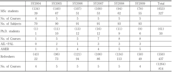
The numbers of students who are enrolled and
Table 1. Summary of numbers of completed students in OU-NANOPROGRAM. The numbers in parentheses are those of registered students.
SY2004 SY2005 SY2006 SY2007 SY2008 SY2009 Total
MSc students (134) 39
(140) 67
(107) 51
(100) 53
(94) 62
(78) 55
(653) 327
No. of Courses 4 5 5 5 5 5
No. of Subjects 70 90 91 91 93 93
Ph.D. students (1) 1
(11) 10
(13) 12
(16) 12
(11) 9
(9) 6
(61) 50
No. of Courses 1 5 5 7 8 8
AIL-PAL 0 2 1 3 3 3
AMER 1 3 4 4 5 5
Refreshers (43)
22
(96) 73
(121) 94
(106) 86
(134) 113
(50) 49
(550) 437
No. of Courses 4 5 5 5 5 4 (1264)
814 AIL-PAL: Academia-Industry-Liaison Project Aimed Learning & Training, AMER: Advanced Multidisciplinary Exploratory Research
completed the MSc, PhD and refresher course pro- grams are summarized in Table 1 during SY (Scholar Year)2004 and SY2009. In the following section, we give a more detailed description of the OU-NANO- PROGRAM [1-4].
1. MSc. COURSE
New courses under the OU-NANOPROGRAM are prepared as one-year minor courses (subsidiary pro- grams) for MSc. They are divided into five courses:
1) Computational NanoMaterials and NanoDevice Design (e.g., Quantum Simulations, Ab-Initio Quantum-Based Computational Materials Design) 2) NanoElectronics and NanoMaterials (e.g., Quan-
tum Electronics, Quantum Functional Materials, Quantum Nano-Devices, Nanoprocessing Tech- nology)
3) SupraMolecules and NanoBioprocesses (e.g., Supramolecule Synthesis and Functionalization, Biomechanics and Functions)
4) NanoStructure Characterization and Analyses (e.g., Characterization and Imaging, Electron and
Probe Microscopy)
5) NanoPhotonics (e.g., Ultra-High Resolution Imaging, Quantum Optical Devices, Optical Sensing, Quantum Informatics)
All the above-mentioned courses consist of a series of lectures and hands-on practices conducted by the lecturers and researchers belonging to six graduate schools (viz., Graduate Schools of Science, Medicine, Pharmacy, Engineering, Engineering Science, and Frontier Biosciences) and six research institutes and centers (viz., Institute of Scientific and Industrial Research, Joining and Welding Research Institute, Institute of Laser Engineering, Research Center for Ultra-High Voltage Electron Microscopy, Research Center for Quantum Science and Technology under Extreme Conditions, and Research Center for Solar Energy Chemistry).
In order to complete the OU-NANOPROGRAM course, from more than 90 subjects offered (corresponding to 2 academic units each), students are required to take at least 8 academic units. In addition, the students should also pass a compulsory intensive hands-on train- ing course, which last for 3∼5 days with using advanced
research instruments such as computer clusters, scan- ning/tunneling electron microscope (SEM/TEM), con- focal laser microscopes, electron lithography apparatus, allowing the students to design, fabricate, measure, characterize, and functionalize nanomaterials and nanodevices.
The most characteristic lecture in MSc. program is Nanotechnology Career-up Lecture opened in 2007 as compulsory subject. It consists of series of omnibus lectures and 15 researchers and engineers working in nano-related industries and institutions introduce various kinds of their knowledge and experiences on the application of nanotechnology, such as cost per- formance, societal implication, public engagement, entrepreneurship, intellectual property, business model, etc. It is quite useful for the students to be more familiar to various kinds of practical applica- tion in nanotechnology. About 100 students take this course every year.
2. Ph. D. COURSE
There are two kinds of one-year courses: the Academia-Industry Liaison Project-Aimed Learning (Liaison-PAL) Education/Training course and the Advanced Multi-Disciplinary Exploratory Research (AMER) Training course. The aim of this program is to produce fresh and career-advanced PhD graduates, who are interested in nanoscience and nanotechnology fields other than their own field of specialization, and have the way of thinking appropriate in industry or in academe with the ability of working efficiently and harmoniously in collaboration with researchers and en- gineers in other fields of discipline.
In the Liaison-PAL training course, a team of students (3∼5) members work hand-in-hand on a particular R&D project, for one year, under the guidance of designated research coordinators from the industry and the academe. The students learn not only the importance of industrial way of thinking but also public engagement,
nano risk, standardization and nanocommunication. Up to now, there are four topics offered, viz.,
∙Exploring the physical properties of nano-mate- rials fabricated in supercritical fluid
∙MEMS (Micro-Electro-Mechanical Systems) tech- nology for medical sensors and bio-actuator applications.
∙Electroluminescent organic nano-structured and thin film devices - electronic and optical prop- erties
∙Organic nano-particle pigment film - structures and optical property.
The studies are being carried out in collaboration with electric and chemical companies and include a variety of practices, such as brain storming, project planning, practice, internship, presentation and publication or patent preparation, public implication, nanocommuni- cation, etc. It is rather hard for the students, but very much motivated for social practice and job-hunting.
The students experience industrial ways of thinking and public implication.
In the AMER training course, a student undergoes one-year research training under a guidance of faculty member assigned from a different department and field.
The students present and defend their research activity before a designated evaluation committee. There are five topics offered to the students, viz.,
∙Nanomaterials and device design with using computational design techniques,
∙Measurement and characterization of nano- materials and their functionality by means of transmission electron microscopy
∙Fabrication and physical and optical character- ization of periodically-poled dielectric nano- materials
∙Fabrication of nanostructures with using elec- tron beam lithography
∙Bio-imaging by means of confocal two-photon microscope and Raman microscope
Three or four students from different fields form
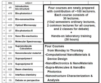
Figure 3. Typical example of the syllabus in refresher program.
one group to share their sub-subjects depending on their own specialties. It is very much motivated for multidisciplinary thinking.
3. REFRESHER COURSE
On October 2004, Osaka University extended the in- ter-/trans-disciplinary graduate program on naand nanotechnology to graduate-level recurrent (refresher) courses in the form of weekday night school which are offered to young researchers working in nano- technology-related industries. This one-year-long program is prepared in anticipation of the emerging needs of young researchers in industries, who are cur- rently (or will be in the near future) working in nano- technology-related fields. The courses offered under this program bore the same course name as the five courses offered in the MSc. course program up to SY2008 and reduced to 4 courses by combining the third and fifth courses. Each course consists of 30 weekly lectures of 3 hours, held at Osaka University NAKANOSHIMA Campus located at the heart of Osaka city in the form of TV distance education through internet, and has been broadcasted live to, at most, 14 satellite classrooms lo- cated in major cities in Japan. Currently, 5 satellite classrooms have been located in the west Japan; 3 in the middle Japan, 3 in Tokyo, and 3 in the north-east Japan. The enrolled part-time refresher students are permitted to set up their own tailor-made program, depending on their individual needs, under the guidance of the course coordinator. Upon completion of the re- quirements, i.e., attendance of all class lectures and the corresponding intensive hands-on training sessions, held for 3∼5 days, the students receive an officially stamped Certificate of Completion of the program from Osaka University under the name of the university presi- dent and acquire official 9 credits of graduate school.
The young researchers in the industries not only know the researchers and the research activities in Osaka University, but also form new networks, personal and/or
professional among them. Each lecture is digitally re- corded and can be viewed through streaming e-learning/
webcasting through internet. The example of the syllabus for the third course is shown in Fig. 3.
In order to fit with industrial demand, the Academia- Industry Liaison Consortium (ALICE-ONE) gives useful advice and suggestion for improving the program and financially supporting the students with the scholar- ship.
4. SPECIAL LECTURES AS COMMON SUBJECTS FOR GRADUATE AND REFRESHER PROGRAMS
There are two kinds of special lectures which are aimed for nanocommunication including social, legal and eth- ical relationship and are prepared as common subjects for both graduate students and refresher students:
“Social Engagement on Nanotechnology” newly started from the spring semester of 2010 and “Road Map Design on Nanotechnology” going to start from the autumn se- mester of 2010, both of which are useful for the develop- ment of nanocommunication among those people who deal with nanotechnology in any respect. The subject of “Social Engagement on Nanotechnology” is specialized in public engagement, risk assessment and admin-
istrative management, standardization, etc., and taught by researchers and government officials working at nano-related institutions, universities, and govern- ment offices. This lecture is organized and conducted by Masafumi Ata of the Advanced Institute for Science and Technology who is one of the Japanese leaders on this subject.
On the other hand, the lecture of “Road Map Design on Nanotechnology” introduces nanoscience and nano- engineering of several important future industrial prod- ucts together with their road maps and deals with neces- sary appliance and public engagement of many kinds of basic elemental engineering in relationship with the specialties of graduate students and engineers working in industry. This lecture is taught by researchers and engineers belonging to the nano-related industries and being engaged in planning the road map for future prod- ucts at the Nanotechnology Business Creation Initiative of Japan (NBCI) where approximately 300 nano-related industries are gathered together for discussion and planning of nano-related subjects.
These special lectures are hold on Saturday and are composed of intensive courses of 15 hours (two days) for “Social Engagement on Nanotechnology” and of 30 hours (four days) for “Road Map Design on Nanotechnology”.
They includes not only the lectures on different subjects given by guest lecturers but also the discussion and debate performed among several small groups composed of the mixing of graduate and refresher students. For the first lecture on “Social Engagement on Nanotechnology”
there were about 70 students gathered together and most of them understood the importance of public engagement on these emerging fields and expressed their con- structive opinion how they practice and develop the pub- lic engagement as their common sense. Next year, new educational system for minor courses will start in Osaka University and it is expected that these special lectures will become compulsory for graduate students who take the minor course of OU-NANOPROGRAM.
Summary
We started the OU-NANOPROGRAM seven years ago for the purpose of education of nanoscience, nanoengineering and nanotechnology and we recog- nized the importance of trans-disciplinary curricu- lum for graduate and refresher students who wish to be engaged in R&D activity with the use of nano- technology. However, nanotechnology is the emerging field and we do not know well the effect of newly emergent nanomaterials on human health and natural environment. Therefore, in order to well develop a variety of products with the use of nanotechnology, it is necessary to pay much attention to public engage- ment, risk assessment, standardization, etc. For this purpose the sense of nanocommunication should be introduced in our OU- NANOPROGRAM. There may be two ways for the development of public engage- ment of nanotechnology, the one is the direct com- munication with general public and the other is the indirect communication through scientists and en- gineers engaged in the development of nano- technology and knowing the importance of public engagement. The former is straightforward but needs the special skill of nanocommunication to make un- derstand well the general people who are not familiar to nanotechnology. The so-called Nanosmile activity [5] conducted by Yves Sicard of UFJ/CEA-Liten and open to public through internet is a typical successful example. On the other hand, the latter is much easier because they are the specialists more or less familiar to nanotechnology, can understand the details more exactly and are expected to become spokespersons of public engagement to the general public. We hope this kind of educational subjects will be more devel- oped in graduate educational systems for the future development of newly emergent fields of science, en- gineering and technology.
Acknowledgments
The authors are grateful to Prof. Shojiro Nishio, Head of the Organization for the Promotion of Research on Nanoscience and Nanotechnology, Osaka University for his continued support and encouragement. This in- novative program was financially supported by the MEXT (Japanese Ministry of Education, Culture, Sports, Science and Technology) Special Coordination Funds for Promoting Science and Technology, through their
“Fostering Talent in Emergent Research Field” program during 2004-2008. It is now continuously supported by the MEXT Special Annual Budget and also by the Osaka University Academia-Industry Liaison Consor- tium for Human Resource Development on Nano Science and Engineering (ALICE-ONE).
References
[1] http://www.sigma.es.osaka-u.ac.jp/pub/nano/pub/nan okiko/html/english.html
[2] T. Itoh, H. Akai, H. Ogawa, W.A. Diño, and S.
Ichikawa, J. Mater. Ed. 28, 15-20, (2006).
[3] T. Itoh, H. Akai, H. Ogawa, W.A. Diño, S. Ichikawa, H. Matsui, M. Ara, and K. Yoshiki, Mater. Res Soc.
Symp. Proc. 931, KK05-09 (2006).
[4] T. Itoh and H. Ogawa, Towards the Practical Application of Nanotechnology ∼Measures for Social Implication∼, ed. M. Ata, Chapter 9, OU-NANOPROGRAM (Gihodo, Tokyo, 2008), pp.263-305 (in Japanese).
[5] Yves Sicard, Nanosmile website, <http://www.
nanosmile.org>.
대학원 수준 교육과 연구 훈련에서의 나노소통 설계
Tadashi Itoha,b*, Hisazumi Akaia,c, Seiji Takedaa,d, Hisahito Ogawaa, Satoshi Ichikawaa, Masaaki Geshia, Masato Araa, and Hirohiko Niiokaa
aThe Institute for NanoScience Design, Osaka University, Toyonaka, Osaka 560-8531
bDepartment of Materials Engineering Science, Osaka University, Toyonaka, Osaka 560-8531
cDepartment of Physics, Osaka University, Toyonaka, Osaka 560-0043
dThe Institute of Scientific and Industrial Research, Osaka University, Mihogaoka 8-1, Ibaraki, Osaka 567-0047
(2010년 7월 1일 받음, 2010년 10월 8일 수정, 2010년 10월 11일 확정)
나노과학, 나노공학, 및 나노기술의 축적된 지식을 대중참여라는 관점을 첨가하여 대학원생이나 젊은 과학자들에게 가르치기 위하여, 오사카 대학은 2004년부터 다양한 교육 및 훈련 프로그램을 제공하고 있는데, 교학문적(交學問的) 대학원 부전공 과 목, 야간 강좌, 단기 국제훈련 프로그램 등이다. 연속강의는 위성통신을 이용하여 교실에 전달되기도 한다. 또한 학생들은 현 대시설을 활용한 실습을 통하여 직접, 나노소재와 나노소자를 설계, 제작, 측정, 특성분석 및 기능화 할 수 있다. 그리고 특별 히 사회적, 법적, 윤리적 관계를 포함하는 나노소통에 관한 연구훈련 프로그램과 강좌 시리즈가 네 개 개설되어 있으니, “나 노기술 경력 건설 강좌”, “나노기술의 대중 참여”, “나노기술 지도 설계”, “목적과제 학습 및 훈련 프로그램(PAL)”이다. 전체 프로그램의 윤곽이 나노소통 특별 프로그램과 함께 소개되어 있다.
주제어 : 나노과학, 나노공학, 나노기술, 대학원 수준 교육, 연구 훈련, 대중 참여, 나노소통
* [전자우편] [email protected]