ISSN: 1226-7244 (Print) ISSN: 2288-243X (Online) 논문번호 16-02-09
52
j.inst.Korean.electr.electron.eng.Vol.20,No.2,174∼176,June 2016 http://dx.doi.org/10.7471/ikeee.2016.20.2.174
체온 이용이 가능한 나노입자 박막 열전소자의 플랫폼 개발연구
Design of the Platform for a Nanoparticle thin Film
Thermoelectric Device transforming Body Heat into Electricity
양승건*, 조경아*, 최진용*, 김상식*★
Seunggen Yang*, Kyoungah Cho*, Jinyong Choi*, Sangsig Kim*★
Abstract
In this study, we maximize the temperature difference between the ends of a HgTe nanoparticle(NP) thin film on a thermoelectric platform with a through-substrate via. The thermoelectric characteristics of the HgTe NP thin film show p-type behavior and its Seebeck coefficient is 290 μV/K. In addition, we demonstrate the possibility of wearable thermoelectric devices transforming body heat into electricity from through-substrate via thermoelectric platforms on human skin.
요 약
본 연구에서는 HgTe 나노입자 박막 수평열전 플랫폼에 via를 형성하여 나노입자 박막 양단의 온도 차이를 극대 화하였다. HgTe 나노입자 박막은 p-type의 열전 특성을 보였으며, HgTe 나노입자 박막 수평열전소자에서 제백계 수는 290 μV/K이였다. 또한 피부 위의 via 열전 플랫폼을 통해서 향후 차세대 웨어러블 전자 소자의 구현 가능성을 확인하였다.
Key words : Via, thermoelectric, HgTe, nanoparticles, plastic substrates
* Dept of Electrical Engineering, Korea University
★
Corresponding author
e-mail : [email protected], tel:02-3290-3245
※ Acknowledgment
This work was partly supported by the National Research Foundation of Korea (NRF) Grant funded by the Korean Government (MSIP) (No. NRF-2013R1A2A1A03070750 and NRF-2015R1A2A1A15055437); National Research Foundation of Korea (NRF) Grant funded by the Korean Government (MSIP) (No.
NRF-2015R1A5A7037674); Basic Science Research Program Through the National Research Foundation of Korea (NRF) funded by the Ministry of Education (NRF-2015R1D1A1A01057641); R&D program of MOTIE/KEIT. [10054570, Highly educated human resources development project on cutting-edge sensor technology for sensor industry acceleration]; Brain Korea 21 Plus Project in 2016, and a Korea University Grant.
Manuscript received Mar, 30, 2016; revised Jun, 7, 2016 ; accepted. Jun, 10, 2016
This is an Open-Access article distributed under the terms of the Creative Commons Attribution Non-Commercial License (http://creativecommons.org/licenses/by-nc/3.0) which permits unrestricted non-commercial use, distribution, and reproduction in any medium, provided the original work is properly cited.
(174)
Design of the Platform for a Nanoparticle thin Film Thermoelectric 53 Device transforming Body Heat into Electricity
Ⅰ. 서론
최근 다기능 웨어러블 전자 소자의 구현을 위 해서 지속적인 전력공급이 가능한 에너지 소자에 대한 관심이 증가하고 있다 [1,2]. 다양한 열전 반도체 나노물질 소재 중에서, 나노입자 박막은 전기전도도와 열전도도의 독립적인 조절을 통해 고효율 열전 발전의 가능성을 보여주고 있다 [3,4]. 그러나 나노입자 박막은 수평구조로만 제 작이 가능하여, 열전에 필수적인 온도 차이를 체 온으로 얻기에는 어려움이 있다. 이를 해결하기 위해서는 수평열전소자에서 온도 차이를 극대화 할 수 있는 플랫폼 개발이 중요하다. 따라서 본 연구에서는 수평열전소자의 플랫폼에서 하나의 전극 쪽에 via를 뚫어 나노입자 박막 양단의 온 도 차이를 극대화시키고자 한다. 또한 향후 체온 을 통한 웨어러블 전자 소자의 구현 가능성에 대 해서 알아보고자 한다.
Ⅱ. 본론
1. 실험방법
본 연구에서의 나노입자는 콜로이드 방식으로 합성된 HgTe 나노입자를 사용하였다 [5]. 플라스 틱 기판 위에 전동 드릴을 이용하여 400 μm 직 경의 구멍을 뚫은 후, HgTe 나노입자 박막의 열 전 특성 확인을 위한 히터와 E1, E2의 전극, 그 리고 두 전극 사이의 채널에 HgTe 나노입자 박 막을 형성하여 열전 플랫폼을 구성하였고 이는 그림 1에 나타내었다. HgTe 나노입자 박막의 열 전 특성은 Keithley 4200와 IR 카메라 (FLIR-A645SC)를 이용하여 전기적 특성과 온도 측정을 통해 측정하였다. 수평구조 열전플랫폼에 서 온도 차이에 대한 via의 영향을 알아보기 위 해, 프로브 스테이션의 heating stage를 이용하였 다. 본 연구에서의 모든 측정은 대기 중 상온에 서 측정하였다.
Fig. 1. Optical image of the thermoelectric platform 그림 1. 열전 플랫폼의 광학 이미지
2. 결과 및 고찰
제작된 via 열전 플랫폼과 non-via 열전 플랫 폼에서의 전극 E1, E2와 전극 간의 온도 차이 △
TE2-E1의 값을 표 1에 나타내었다. non-via 열전
플랫폼에서의 두 전극에서 보이는 온도차이는 heating stage가 국부적으로 온도가 달라 나타난 것으로, via 열전 플랫폼에서 발생된 두 전극간의 온도 차이와 비교하면 무시할 만한 수준이다.
heating stage의 온도를 60 oC, 80 oC, 90 oC로 증가시킴에 따라 via 열전 플랫폼에서의 △TE2-E1
는 점점 감소하는 것을 확인할 수 있다. 이는 heating stage의 온도가 증가함에 따라서 열이 via 뿐만 아니라 그 주변까지 확산된 결과로 사 료된다.
Table 1. Temperature difference of E1 and E2 in the thermoelectric platform with and without via 표 1. Via 기판과 non-via 기판에서 전극 간의 온도 차이
Heating stage temperature (
oC)
60 80 90
Via substrate
T
E149.24 64.09 75.14 T
E262.38 74.99 81.71
△T
E2-E113.14 10.9 6.57
Non-via substrate
T
E151.27 64.73 71.2
T
E249.16 66.1 72.5
△T
E2-E1-2.11 1.37 1.3
via를 통한 열전달에 따른 △TE2-E1와 그에 따 른 제백 전압을 그림 2에 나타내었다. HgTe 나 노입자 박막의 제백 전압은 양의 값을 갖는 p-type 특성을 보였으며, 그림 2에서의 온도 차
(175)
54
j.inst.Korean.electr.electron.eng.Vol.20,No.2,174∼176,June 2016
이와 제백 전압의 기울기를 통해 290 μV/K의 제 백 계수가 계산되었다.
Fig. 2. The Seebeck voltage as a function of
temperature difference for the HgTe NP thin film 그림 2. HgTe 나노입자 박막의 온도 차이에 따른 제백
전압
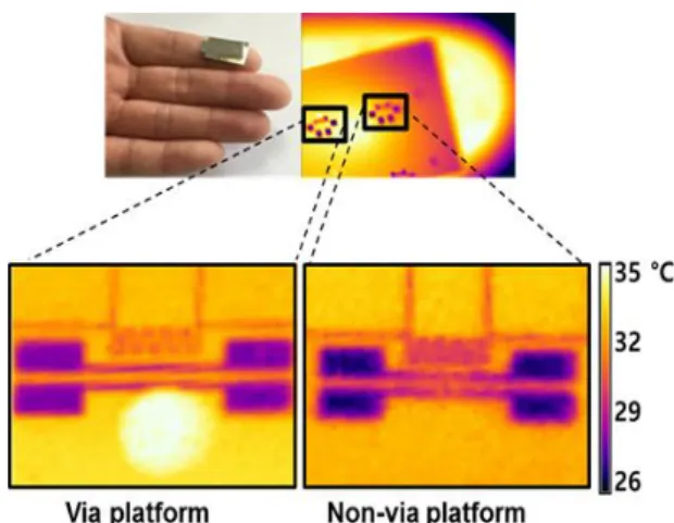
그림 3은 손가락 위에서의 via 열전 플랫폼과 non-via 열전 플랫폼의 온도를 열영상 이미지로 나타낸 그림이다. via 열전플랫폼의 경우 전극 간 의 온도 차이는 2.2 oC였으나, non-via 열전 플랫 폼의 경우는 0.34 oC 온도밖에 차이가 발생하지 않았다. 열전특성이 우수한 나노입자 박막의 수 평열전소자를 웨어러블 열전소자로 활용하기 위 해서는 via를 이용한 열전플랫폼이 유용하다는 것을 확인하였다.
Fig. 3. IR image of the thermoelectric platform on the skin
그림 3. 피부 위에서의 열전 플랫폼 열영상 이미지
Ⅲ 결론
본 연구에서는 플라스틱 기판 위에 via 형성 후 HgTe 나노입자 박막의 열전 특성을 확인하였 다. 기판에 via를 형성함으로서 전극 간의 온도 차이를 극대화시키고 이를 통해 향후 차세대 웨 어러블 전자 소자의 구현 가능성을 확인하였다.
References
[1] V. Leonov, T. Torfs, C. V. Hoof and R. J.
M. Vullers, “Smart Wireless Sensors Integrated in Clothing:an Electrocardiography System in a Shirt Powered Using Human Body Heat”, Sens.
Transducers J., 107, p. 165, 2009
[2] E. J. Yoon, J. T. Park and C. G. Yu,
"Thermoelectric Energy Harvesting Circuit Using DC-DC Boost Converter", Journal of IKEEE, 3, p. 284, 2013
[3] M. R. Dirmyer, J. Martin, G. S. Nolas, A.
Sen and J. V. Badding, “Thermal and Electrical Conductivity of Size-Tuned Bismuth Telluride Nanoparticles”, small, 5, p. 933, 2009
[4] K. Ariga, M. Li, G. J. Richards and J. P.
Hill, “Nanoarchitectonics: A Conceptual Paradigm for Design and Synthesis of Dimension-Controlled Functional Nanomaterials”, J. Nanosci. Nanotechnol., 11, p. 1533, 2011 [5] H. Seong, K. Cho and S. Kim, “Photocurrent characteristics of solution-processed HgTe nanoparticle thin films under the illumination of 1.3 μm wavelength light”, Semicond. Sci.
Technol., 23, p. 075011, 2008