• 검색 결과가 없습니다.

Rapid Fabrication of Cu/Cu<sub>2</sub>O/CuO Photoelectrodes by Rapid Thermal Annealing Technique for Efficient Water Splitting Application

N/A
N/A
Protected

Academic year: 2021

Share "Rapid Fabrication of Cu/Cu<sub>2</sub>O/CuO Photoelectrodes by Rapid Thermal Annealing Technique for Efficient Water Splitting Application"

Copied!
7
0
0

로드 중.... (전체 텍스트 보기)

전체 글

(1)

Rapid Fabrication of Cu/Cu 2 O/CuO Photoelectrodes by

Rapid Thermal Annealing Technique for Efficient Water Splitting Application

Minjeong Lee

1

, Hyojung Bae

2

, Hokyun Rho

3

, Vishal Burungale

2

, Pratik Mane

1

, Chaewon Seong

1

, and Jun-Seok Ha

1,2,3,†

1

Department of Advanced Chemicals & Engineering, Chonnam National University, 77 Yong-bong-ro, Buk-gu, Gwangju 61186, Korea

2

Optoelectronics Convergence Research Center, Chonnam National University, 77 Yong-bong-ro, Buk-gu, Gwangju 61186, Korea

3

Energy Convergence Core Facility, Chonnam National University, 77 Yongbong-ro, Buk-gu, Gwangju 61186, Korea (Received November 30, 2020: Corrected December 7, 2020: Accepted December 8, 2020)

Abstract: The Cu/Cu

2

O/CuO photoelectrode has been successfully fabricated by Rapid Thermal Annealing technique.

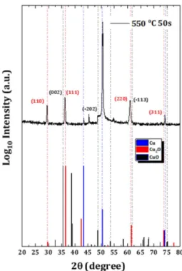
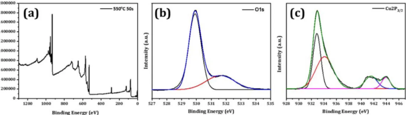
The structural characterization of fabricated photoelectrode was performed using X-Ray diffraction, while elemental com- position of the prepared material has been checked with X-Ray Photoelectron Spectroscopy. The synthesis parameters are optimized on the basis of photoelectrochemical performance. The best photoelectrochemical performance has been observed for the Cu/Cu

2

O/CuO photoelectrode fabricated at 550

o

C oxidation temperature and oxidation time of 50 sec- onds with highest photocurrent density of -3 mA/cm

2

at -0.13 V vs. RHE.

Keywords: Cu, Cu

2

O, CuO, Oxidation, Photoelectrode, Water splitting

1. Introduction

The ever-increasing demand of energy in recent decades is causing very severe environmental effects such as abnor- mal climates, enormous pollution and the most important one is large amount of carbon dioxide emission, which is ultimately responsible for the global warming.

1)

Therefore, it is a need of time to look for some new energy source which can substitute the current conventional energy sources and at the same time it shouldn’t cause any envi- ronmental issues. Among eco-friendly energy sources, the sun is constantly emitting a huge amount of energy, about 174 PW of solar energy reaches the Earth's atmospheric surface, this corresponds to about one-two-billionth of the total radiant energy emitted by the sun. If light energy can be utilized as a new energy source, the problem of environ- mental pollution and the problem of energy depletion due to excessive use of fossil fuels can be solved. There are many ways to make light energy available as chemical energy without generating carbon dioxide. Photoelectro- chemical (PEC) cells with active semiconductor electrolyte junction are considered to be efficient solar energy har- vester and intensive research is going on, to use such sys-

tems in photo assisted water splitting for the production of hydrogen which is a much cleaner substitute of fossil fuels.

2,3)

Hydrogen can replace existing fossil fuels with high energy density (143 MJ kg

−1

).

4)

In addition to this, when used as an energy source, water, which is a benign by- product, is produced, and therefore, it has the advantage of having no environmental impact even when used in large quantities.

5)

PEC does not require complicated equipment or conditions, and it has the advantage of low cost because it can carry out reduction reaction by utilizing the potential difference between the two electrodes as long as it has a simple electrical device or electrolyte. Besides, using the sunlight to split water and produce hydrogen is worth developing in several ways to produce energy because both water and sunlight are abundant. Since Edmond Becquerel discovered the photoelectric effect, research has been ongoing to convert the sun into electrical and chemical fuels.

6)

A target is to utilize the infinite solar energy as electric power, hydrogen, etc., which is energy that can be used.

7)

In order to use a semiconductor substance as a photo- electrode in PEC, the oxidation-reduction level of water

Corresponding author E-mail: [email protected]

© 2020, The Korean Microelectronics and Packaging Society

This is an Open-Access article distributed under the terms of the Creative Commons Attribution Non-Commercial License(http://creativecommons.org/

licenses/by-nc/3.0) which permits unrestricted non-commercial use, distribution, and reproduction in any medium, provided the original work is

properly cited.

(2)

decomposition and hydrogen production reaction must be included in the band gap.

8)

Fujishima and Honda reported, for the first time, the possibility of using TiO

2

in PEC split- ting of water, but, on account of large band gap of TiO

2

(3.1 eV), the conversion efficiency of solar energy was limited.

9)

Cu

2

O, on the other hand, is a p-type semiconduc- tor with a band gap of 2.0-2.2 eV, this is nontoxic, and is used for PEC hydrolysis with high efficiency under sun- light at an inexpensive and appropriate band gap position (0.7 V lower than the band gap required for hydrolysis).

10)

In addition to this, as compared to other electrodes copper oxide is more capable of selectively producing hydrocar- bons from CO

2

with reasonable Faradaic Efficiency at ambient conditions of temperature and pressure.

11)

However, Cu

2

O is very vulnerable to photocorrosion, due to which there is a big issue of stability with this material. At the same time other form of copper oxide i.e. CuO is more sta- ble as compared to Cu

2

O and these two materials also form Type II band alignment with each other. This Type II band alignment is very useful when such combination of Cu

2

O/

CuO heterojunction is being used as photoelectrode in Pho- toelectrochemical cells for water splitting application.

12)

In this scenario, the present work focused on the optimi- zation of the experimental conditions for the rapid synthe- sis of Cu/Cu

2

O/CuO photoelectrode from Cu foil using Rapid Thermal Annealing (RTA) technique in order to get good photoelectrochemical performance. The experimental parameters are optimized in such a way that formed Cu

2

O will be completely covered by the protecting layer of CuO.

2. Experimental Details

2.1 Preparation of Cu/Cu

2

O/CuO Electrode

The starting substrates were Cu foil (99.95%, Alfa Aesar). The Cu substrates were rinsed using 1:1 HCl(aq).

Cu foils were oxidized for 30 seconds by RTA (Korea vac- uum tech) at 1.5 SLPM, N

2

atmosphere, 500

o

C ~ 600

o

C temperature to check the effect of temperature. After that, at 550

o

C, Cu foils were oxidized for 30 ~ 60 seconds for checking the effect of oxidation time. The actual electrode is made up of Cu/Cu

2

O/CuO foils of size 1×1.5 cm

2

, Tef- lon coated Cu wire was soldered on the foil to make ohmic contact. Further these electrodes were covered with epoxy in such a way that only 1×1 cm

2

area will be exposed. After that, the epoxy was allowed to dry for a day.

2.2 Material Characterization:

The phases and crystalline structure of Cu/Cu

2

O/CuO electrodes were characterized using X-ray diffraction with

an X-ray diffractometer (XRD, PANalytical, X'Pert PRO MPD). The chemical states of the elements were deter- mined by X-ray photoelectron spectroscopy (XPS, K- ALPHA+, High-Performance X-ray Photoelectron Spec- troscopy). Field Emission Scanning Electron Microscope (JSM-7500F, Oxford Instruments) was used for examining surface morphology of deposited samples.

2.3 Electrochemical Characterizations:

PEC properties were measured in a three-electrode con- figuration using a PARSTAT 4000 (AMETEK Princeton Applied Research) potentiostat. A PEC cell consisting of Ag/AgCl/KCl as the reference electrode (RE), Pt wire as the counter electrode (CE), and the sample film as the working electrode. The electrolyte was 0.1M NaOH. A simulated light of 100 mW/cm

2

was used for the illumina- tion. The photocurrent density was calculated by dividing the measured photocurrent by the area of the electrode. The potential values were transformed to the reversible hydro- gen electrode (RHE) scale as follows:

V

RHE

= V

Ag/AgCl/KCl

+ 0.201 + 0.059 pH.

3. Results and Discussion

3.1 X-ray Diffraction Study

Fig. 1 shows X-ray diffraction patterns of Cu/Cu

2

O/CuO sample prepared with 550

o

C oxidation temperature and 50

Fig. 1. X-Ray diffraction pattern of Cu/Cu

2

O/CuO electrode

prepared with 550

o

C temperature and 50 seconds oxidation

time.

(3)

seconds time. The X-Ray diffraction pattern is well matched with the JCPDS cards 04-0836 (Cu), 01-077-0199 (Cu

2

O) and 45-0937 (CuO), which confirms the presence of both Cu

2

O and CuO on the Cu substrate. Cu

2

O has cubic structure while CuO has monoclinic structure.

3.2 X-Ray Photoelectron Spectroscopy

The graphs related to XPS measurements are shown in Fig. 2. Fig. 2(a) shows the survey spectrum of sample pre- pared with 550

o

C oxidation temperature and 50 seconds of oxidation time. Fig. 2(b) shows narrow scan spectra of O1s, where peak near to 530 eV binding energy is due to the Cu-O bond present in the sample while the peak near to 532 eV is surface hydroxides. Fig. 2(c) shows the narrow scan spectra of Cu2P

3/2

, in this spectrum the peak at 932.88 eV binding energy is associated with Cu2P

3/2

for Cu

2

O, while the peak at 934.12 eV with two satellite peaks at 941.50 eV and 943.44 is associated with Cu2P

3/2

for CuO.

12)

Fig. 3 shows the XPS depth profile of 550

o

C, 50 sec-

onds sample. At the surface, due to the CuO layer, Cu and O are present in approximately the same ratio while below this layer, there is the Cu

2

O, so the percentage of Cu is increased and percentage of O is decreased. After this, only a large amount of Cu and a small amount of O are present.

Therefore, the presence of both Cu

2

O and CuO has been confirmed from this study.

3.3 Scanning Electron Microscopy

Figure 4 a) shows SEM images of Cu and Cu/Cu

2

O/CuO electrodes prepared with 500

o

C, 550

o

C, and 600

o

C of oxidation temperature and time of 30s. From the figure, it is observed that the surface of the Cu foil becomes rougher and rougher with increasing oxidation temperature, which is obvious since with increasing temperature the rate of oxidation is also increased.

Fig. 4(b) shows SEM images of Cu/Cu

2

O/CuO elec- trodes prepared with 550

o

C, oxidation temperature, and time of 30s, 40s, 50s, and 60s. From the figure it is observed that the surface roughness is also increased with increasing oxidation time, this is because as time passes more and more surface layers of Cu foils get oxidized. In the SEM image of the sample prepared with 550

o

C of oxi- dation temperature and 60s of oxidation time, it is observed that some part of the superficial oxidized layer is started stripping out from the Cu substrate. So, the overall study of the surfaces of the oxidized samples suggests that the oxi- dation time for preparing Cu/Cu

2

O/CuO at 550

o

C should be 50s or less since after this time the stripping of film from the Cu substrate starts.

3.4 Photoelectrochemical Performance

The Fig. 5 shows LSV plots of Cu/Cu

2

O/CuO electrodes oxidized at different temperatures (i.e. 500

o

C, 550

o

C and 600

o

C respectively). From the figure it is observed that the onset potential was not changed much all three samples i.e.

Fig. 2. (a) Survey spectrum of 550

o

C 50 seconds sample (b) O1s XPS spectra of Cu/Cu

2

O/CuO electrodes for 550

o

C temperatures (c) Cu2P

3/2

XPS spectra of Cu/Cu

2

O/CuO electrodes for 550

o

C temperatures.

Fig. 3. Depth profiling of a Cu/Cu

2

O/CuO electrodes for 550

o

C

50 seconds showing the O, Cu evolution as the function of

etching time, where etching begins at the air/film interface.

(4)

there is no substantial effect of oxidation temperature on the onset potential, which is around +0.6 V vs. RHE for all samples. In the case of photocurrent, there is not much change is observed in very low bias region (i.e. below 0.3 V vs RHE), however, it has been changed substantially in higher bias region. Specifically, the Cu/Cu

2

O/CuO elec- trode prepared at 500

o

C has highest photocurrent in the

bias region of 0.3 V to 0.0 V vs RHE while in a very high bias region (above 0.0 V) the Cu/Cu

2

O/CuO electrode pre- pared at 550

o

C has the highest photocurrent. The electrode prepared at 600

o

C has overall low photocurrent for all ranges of applied bias. From LSV plots in Fig. 5 it is also observed that prominent transient photocurrent spikes are only present in the case of samples prepared at 550

o

C and Fig. 4(a). SEM images of Cu and Cu/Cu

2

O/CuO electrodes prepared with 500

o

C, 550

o

C, and 600

o

C oxidation temperature and time

of the 30s.

Fig. 4(b). SEM images of Cu/Cu

2

O/CuO electrodes prepared with 550

o

C, oxidation temperature and time of 30s, 40s, 50s, and 60s.

(5)

600

o

C while those are not much prominent in case of sam- ple prepared at 500

o

C.

Scheme 1 and Scheme 2 are given below to discuss the mechanistic details regarding the change in photoelectro- chemical performance of the above samples. The presence of photocurrent spikes only in the lower bias region can be

explained with the help of Scheme 1. As given in Scheme 1(a) at low bias condition there is low band bending at electrode/electrolyte interface due to which surface states are above the fermi energy level of the semiconductor and hence they are empty. When this p-type semiconductor is illuminated with light, photogenerated electrons move toward the electrode surface while photogenerated holes move towards external contact made on the other side of the electrode. During this journey, electrons are getting trapped in this empty surface states and they recombine with available holes giving rise to recombination losses.

However, in the case of higher bias condition (Scheme 1(b)), there is high band bending, due to which surface states goes below the fermi energy level and hence they are filled. So, when the semiconductor is illuminated, no recombination occurs due to these surface states.

It is well known that when heated, Cu firstly oxidized into Cu

2

O at low temperatures and then gradually con- verted into CuO when the temperature goes above 200

o

C.

13)

In the present case the temperature transition rate is very fast hence this process of conversion of Cu to Cu

2

O and then to CuO takes place very rapidly and during this process, there is good probability that a number of defects will also be introduced especially in the case of Cu

2

O to CuO conversion. In the same scenario, the pres- ence of photocurrent spikes observed in the case of sam- ples prepared at higher temperatures i.e. 550

o

C and 600

o

C suggests that there are more surface states or defects in these samples as compared to the sample pre- pared at 500

o

C. The good photocurrent of the sample pre- pared at 500

o

C in bias region 0.3 V to 0.0 V is may be due to the more amount of Cu

2

O present in this sample as com- pared to other samples. As discussed earlier if the amount of CuO is related to the number of defects then the absence of prominent photocurrent spikes can easily be justified in the case of sample deposited at 500

o

C. The good PEC per- formance of the sample prepared at 550

o

C at the highest bias region is may be due to the formation of Type II band alignment between Cu

2

O and CuO which provides an addi- tional driving force for the separation of photogenerated charge carriers. The reason for the low photocurrent of this sample in lower bias region as compared to the 500

o

C sample is because in the lower bias region recombination due to surface states is dominant while in the higher bias region effect of these surface states is nullified. As shown in Scheme 2, when the temperature is increased above 550

o

C, the copper oxide layer becomes fragile and become less adherent to Cu substrate and at 600

o

C some part of the film also started stripping off. This causes large Fig. 5. Linear Sweep Voltammetry plots of Cu/Cu

2

O/CuO elec-

trodes prepared at 500

o

C, 550

o

C, 600

o

C temperatures.

Scheme 1. Schematic illustration of the band structure near the surface of Cu/Cu

2

O/CuO electrode in contact with an electrolyte. (a) low bias potential (b) high bias potential

Scheme 2. Schematic of Cu/Cu

2

O/CuO electrode structure oxidized

at 500

o

C, 550

o

C, 600

o

C 30 seconds.

(6)

increment in the resistance at the interface of the Copper Oxide layer and Copper. This is the reason that the sample prepared at 600

o

C shows overall less photocurrent as com- pared to other samples. The defects in the copper oxide films can be eliminated by increasing crystallinity of the sample and this crystallinity can be improved by increasing oxidation time. So, to check effect of increased oxidation time on the photoelectrochemical performance, the oxida- tion temperature of 550

o

C has been chosen, since this film has shown the highest photocurrent density of -2.5 mA/

cm

2

at -0.13 V vs. RHE which higher than other elec- trodes. The lower photocurrent of this film in the lower bias region is mainly due to surface states which are due to defects and these defects can easily be passivated by increasing the crystallinity of this sample.

Fig. 6 shows LSV plots of Cu/Cu

2

O/CuO electrodes oxi- dized at 550

o

C for different oxidation times (i.e. 30, 40, 50 and 60 seconds respectively). From figure it is observed that there is no change in onset potential due to change in oxidation time which is around +0.6 V vs. RHE for all

samples. The photocurrent is also almost same in the lower bias region i.e. below +0.3 V vs. RHE but it is increased in the region above +0.3 V vs. RHE with time up to 50 sec- onds and again photocurrent decreased for the sample pre- pared with 60 seconds of oxidation time. The photocurrent in the case of this sample is well below the photocurrent of the sample prepared at 30 seconds. From Fig. 6 it is also observed that the only sample prepared at 40 seconds has prominent photocurrent spikes in the low bias region, which means that only this sample has significant number of surface states or defects as compared to other samples.

This variation in the photocurrent can be easily understand with the help of Scheme 3.

As shown in scheme 3, with and increase in oxidation time the chunks of CuO forming in between Cu

2

O layer also goes on increasing. Around 50 seconds of oxidation time almost the whole surface of Cu

2

O gets covered with newly formed CuO and perfect heterojunction of Type II band alignment formed everywhere on the surface of the film. Further increment in the oxidation time causes the weakening of adherence between Cu substrate and Copper oxide layers and these layers started stripping off from the substrate. Hence, the best PEC performance with photocur- rent density of -3 mA/cm

2

at -0.13 V vs. RHE has been observed for the sample prepared with oxidation time of 50 seconds. The prominent photocurrent spikes in the case of samples prepared with 40 seconds of oxidation time are may be due to a large number of CuO chunks as compared to other samples, while less dominant spikes observed in case of 50 and 60 seconds are may be because 50 seconds is enough time for overall crystallization of CuO chunks in the form of uniform layer over the base layer of Cu

2

O. The decrement observed in the case of the sample prepared with 60 seconds oxidation time is may be due to the strip- ping of film from the substrate, which causes an increment in the interfacial resistance between Copper oxide and Cu.

Fig. 6. Linear sweep voltammetry graph referenced to the RHE electrode of Cu/Cu

2

O/CuO electrodes at 550

o

C 30, 40, 50, 60 seconds

Scheme 3. Schematic of Cu/Cu

2

O/CuO electrode structure oxidized at 550

o

C for 30, 40, 50, 60 seconds.

(7)

The tentative band diagram of the Cu/Cu

2

O/CuO combi- nation has been shown in Scheme 4. This Type II band alignment allows the effective transfer of photogenerated electrons from the conduction band of Cu

2

O towards the conduction band of CuO and then to the electrolyte, while photogenerated holes are effectively transferred from the valence band of CuO towards the valence band of Cu

2

O.

As discussed earlier the Cu

2

O has good photoelectrochem- ical properties than of CuO, because Cu

2

O is a direct band- gap material while CuO is an indirect bandgap material.

Due to this fact photogeneration of electrons and holes is high in Cu

2

O as compared to CuO but at the same time rate of recombination of this photogenerated charge carries is also high. In the case of CuO the probability of recombina- tion is relatively low because of its indirect bandgap, where transition of charge mainly involves phonons. In addition to this due to the narrower bandgap of CuO, this combina- tion of Cu

2

O/CuO also contributes significantly to expand the absorption of the solar spectrum.

4. Conclusion

The parameters for the rapid fabrication of Cu/Cu

2

O/

CuO photoelectrode has been successfully optimized. It is observed that to fabricate good film of Cu

2

O and CuO without stripping on the Cu substrate the oxidation tem- perature should be 550

o

C or less and the time should not be more than 50 seconds for this much high temperature.

The best photoelectrochemical performance has been observed for Cu/Cu

2

O/CuO photoelectrode fabricated at 550

o

C oxidation temperature with oxidation time of 50 seconds with highest photocurrent density of -3 mA/cm

2

at -0.13 V vs. RHE.

Acknowledgement

This research was supported by Priority Research Cen- ters Program through the National Research Foundation of Korea (NRF) funded by the Ministry of Education, Science and Technology (2018R1A6A1A03024334) and the Basic Science Research Capacity Enhancement Project through the Korea Basic Science Institute (Energy Convergence Core Facility) grant funded by the Ministry of Education.

References

1. H. Kim, H. Bae, S. J. Kang, and J. S. Ha, “MnO

2

co-catalyst effect on Photoelectrochemical Properties of GaN Photoelec- trode”, J. Microelectron. Packag. Soc., 23(4), 113 (2016).

2. S. W. Bang, H. Kim, H. Bae, J. W. Ju, S. J. Kang, and J. S.

Ha, “Improvement of Photoelectrochemical Properties through Activation Process of p-type GaN”, J. Microelectron. Packag.

Soc., 24(4), 59 (2017).

3. Y. S. Chaudharya, A. Agrawala, R. Shrivastava, V. R. Satsan- gib, and S. Dassa, “A study on the photoelectrochemical properties of copper oxide thin fims”, International Journal of Hydrogen Energy, 29(2), 131, (2004).

4. R. K. Ahluwalia and J. K. Peng, “Automotive hydrogen stor- age system using cryoadsorption on activated carbon”, Inter- national Journal of Hydrogen Energy, 34(13), 5476 (2009).

5. T. Bak, J. Nowotny, M. Rekas, and C. C. Sorrell, “Photo-elec- trochemical hydrogen generation from water using solar energy. Materials-related aspects”, International Journal of Hydrogen Energy, 27(10), 991 (2002).

6. E. Bequerel, “Recherches sur les effets de la radiation chimique de la lumie`re solaire, au moyen des courants e´lec- triques”, CR Acad. Sci., 9(145), 1 (1839).

7. M. Grätzel, “Photoelectrochemical cells”, pp.26-32, Materials for Sustainable Energy, (2010).

8. A. Fujishima and K. Honda, “Electrochemical Photolysis of Water at a Semiconductor Electrode”, Nature, 238, 37 (1972).

9. M. A. Khan, M. S. Akhtar, S. I. Woo, and O.-B. Yang,

“Enhanced photoresponse under visible light in Pt ionized TiO

2

nanotube for the photocatalytic splitting of water”, Catalysis Communications, 10(1), 1 (2008).

10. J. Li, X. Jin, R. Li, Y. Zhao, X. Wang, X. Liu, and H. Jiao,

“Copper oxide nanowires for efficient photoelectrochemical water splitting”, Applied Catalysis B: Environmental, 240, 1 (2019).

11. C. Zhao and J. Wang, “Electrochemical reduction of CO

2

to formate in aqueous solution using electro-deposited Sn cata- lysts”, Chemical Engineernig Journal, 293, 161 (2016).

12. J. Han, X. Zong, X. Zhou, and C. Li, “Cu

2

O/CuO photoca- thode with improved stability for photoelectrochemical water reduction”, Rsc Adv., 5(14), 10790 (2015).

13 V. H. Castrejón-Sánchez, A. C. Solis, R. López, C. Encar- nación-Gomez, F. M. Morales, O. S. Vargas, J. E. Mastache- Mastache, and G. V. Sánchez, “Thermal oxidation of copper over a broad temperature range: Towards the formation of cupric oxide (CuO)”, Mater. Res. Express., 6(7), 075909 (2019).

Scheme 4. The band alignment of Cu/Cu

2

O/CuO photoelectrode.

수치

Fig. 1 shows X-ray diffraction patterns of Cu/Cu 2 O/CuO sample prepared with 550 o C oxidation temperature and 50
Fig. 3 shows the XPS depth profile of 550 o C, 50 sec-
Fig. 6. Linear sweep voltammetry graph referenced to the RHE electrode of Cu/Cu 2 O/CuO electrodes at 550 o C 30, 40, 50, 60 seconds

참조

관련 문서