Design of Shielded Encircling Send-Receive Type Pulsed Eddy Current Probe Using Numerical Analysis Method
Young-Kil Shin
Abstract An encircling send-receive type pulsed eddy current (PEC) probe is designed for use in aluminum tube inspection. When bare receive coils located away from the exciter were used, the peak time of the signal did not change although the distance from the exciter increased. This is because the magnetic flux from the exciter coil directly affects the receive coil signal. Therefore, in this work, both the exciter and the sensor coils were shielded in order to reduce the influence of direct flux from the exciter coil. Numerical simulation with the designed shielded encircling PEC probe showed the corresponding increase of the peak time as the sensor distance increased. Ferrite and carbon steel shields were compared and results of the ferrite shielding showed a slightly stronger peak value and a quicker peak time than those of the carbon steel shielding. Simulation results showed that the peak value increased as the defect size (such as depth and length) increased regardless of the sensor location. To decide a proper sensor location, the sensitivity of the peak value to defect size variation was investigated and found that the normalized peak value was more sensitive to defect size variation when the sensor was located closer to the exciter.
Keywords: Encircling Probe, Send-Receive Type, Pulsed Eddy Current (PEC), Numerical Analysis Method
[Received: November 29, 2013, Revised: December 23, 2013, Accepted: December 23, 2013] Department of Electircal Engineeirng, Kunsan National University, Kunsan, Chonbuk, 573-701, Korea ✝Corresponding Author: [email protected]
ⓒ 2013, Korean Society for Nondestructive Testing
1. Introduction
To detect wall thinning or defects of tubes from the outside, an encircling pulsed eddy current (PEC) probe is designed. This noncontact method is expected to offer a rich source of information by providing a deeper penetration than the conventional eddy current testing method due to its broadband nature [1,2]. When bare encircling coils are used in the send-receive type probe, the sensor coil detects not only the magnetic flux produced by induced eddy currents, but also the source magnetic flux.
Eddy current testing is a method that senses magnetic flux affected by eddy currents to detect abnormalities in the test specimen. In order to reduce the influence of the source magnetic flux, a shielded coil is used to prevent a source magnetic flux from directly reaching the sensor coil. Another method uses a
differential arrangement of two sensor coils so that influences of a source magnetic flux are cancelled [3-5]. In this paper, by using the numerical analysis method, a shielded encircling send-receive type PEC probe is designed for aluminum tube inspection and its performance in detecting defects is investigated.
2. Numerical Analysis Method
To predict PEC signals, a transient analysis is required. Therefore, the backward difference method in time was incorporated in this work.
For the spatial analysis of the governing equation, the finite element method was used [3-5]. The governing equation for the PEC testing is
1
s
A J V A
σ t μ
⎛ ⎞
⎛ ⎞ ∂
∇ ×⎜⎝ ∇ × ⎟⎠= − ⎜⎝∇ + ∂ ⎟⎠ (1)
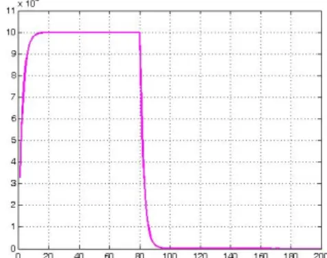
Fig. 1 Input pulse current density (1 time step = 50 s)
0.040 0.05 0.06 0.07 0.08 0.09 0.1 0.11 0.12 0.13 0.14
0.005 0.01 0.015 0.02 0.025 0.03
Fig. 2 Flux distribution at 4 ms
where ,,, are permeability, conductivity, coil current density vector, and magnetic vector potential, respectively. Applying the finite element formulation for space, the following matrix equation is obtained.
[ ]
S A{ } [ ]
C A{ }
Qt
⎧∂ ⎫
+ ⎨⎩∂ ⎬⎭= (2)
where
[ ]
S =∫
vμ1[ ] [ ]
∇N t ∇N dv (3)
[ ]
C =∫
v{ }
N σ[ ]
N dv (4)
{ }
Q =∫
v{ }
N J dvS (5)Here, N is the shape function of a quadrilateral element.
To treat time, the backward difference in time is adopted and the time derivative term is expressed as follows,
{ }
1{ }
1 n n
n A A
A
t t
+ +
∂ −
⎧ ⎫ =
⎨∂ ⎬ Δ
⎩ ⎭ (6)
where {A}n is the magnetic potential evaluated at time, tn.
Rewriting Eq. (2) by using Eq. (6), the following recurrence relation is obtained and the magnetic potential at any time step can be calculated.
[ ] [ ] { }
1{ }
1[ ]{ }
1 n n 1 n
C S A Q C A
t t
+ +
⎡ + ⎤ = +
⎢Δ ⎥ Δ
⎣ ⎦ (7)
The electromotive force induced in the sensor coil, that is the PEC signal, can be calculated as follows.
{ }
n 1{ }
n2emf c
A A
V r
t
π
+ −
= Δ (8)
Where rc is the centroidal radius of the sensor coil element.
3. Numerical Results from Bare Coils
Fig. 1 shows the pulse current density supplied to the exciter coil. The pulse width is 4 ms. The wall thickness and outer diameter (OD) of the aluminum test tube are 1.27 mm and 22.225 mm, respectively. The flux distribution of the encircling exciter coil at 4 ms is shown in Fig. 2. When bare coil sensors are located 0.57, 1.14, and 1.71 OD away from a bare exciter coil (as shown in Fig.
2) around the tube without any defect, the sensor signals from the three locations are calculated and displayed in Fig. 3(a). They show that the peak value of the signal reduces as the sensor is located farther away from the exciter;
but the time to reach the peak value does not seem to change. Therefore, the peak values versus corresponding peak times are compared from a clean tube and tubes with 50% and 75%
deep inner diameter (ID) defects. They are drawn in Fig. 3(b) and it can be seen that the peak time does not change when the sensor distance is between 1.14 OD and 1.71 OD. This
0 20 40 60 80 100 120 140 160 180 200 -8
-6 -4 -2 0 2 4 6 8x 10⁻⁴
Time [1 step = 50 microseconds]
Sensor signals from ferrite shield
0.57D 1.14D 1.71D
(a) Signals from ferrite shielding
0 20 40 60 80 100 120 140 160 180 200
-8 -6 -4 -2 0 2 4 6 8x 10⁻⁴
Time [1 step = 50 microseconds
Sensor signals from carbone steel shield
0.57D 1.14D 1.71D
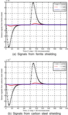
(b) Signals from carbon steel shielding Fig. 5 Shielded sensor signals from a clean tube
with ferrite and carbon steel shielding
is because the magnetic flux generated by the exciter coil arrives directly on the sensor. As a result, the sensor signals are affected significantly by them rather than those from the eddy currents. In eddy current testing, sensors should detect the magnetic flux affected by eddy currents more than those generated by the exciter coil currents. Therefore, in this work, all the coils are shielded in order to avoid detecting source magnetic flux directly. The resulting flux distribution of the ferrite shielded probe at 4 ms is shown in Fig. 4.
0 20 40 60 80 100 120 140 160 180 200
-2.5 -2 -1.5 -1 -0.5 0 0.5 1 1.5 2 2.5x 10⁻³
Time, [1 step = 50 microsecond]
Sensor signal
0.57D 1.14D 1.71D
(a) Sensor signals from three sensor locations
3 3.2 3.4 3.6 3.8 4 4.2 4.4 4.6 4.8 5
0 500 1000 1500 2000 2500 3000
Peak time (x 50μS)
Peak value ( μV)
0.57 D
1.14 D
1.71 D
No defect 50% ID defect 75% ID defect
(b) Peak value vs. peak time
Fig. 3 Signals and the peak value versus peak time from bare coil sensors
0.040 0.05 0.06 0.07 0.08 0.09 0.1 0.11 0.12 0.13 0.14
0.005 0.01 0.015 0.02 0.025 0.03
Fig. 4 Flux distribution of the ferrite shielded probe at 4 ms
4. Numerical Results from Shielded Probe
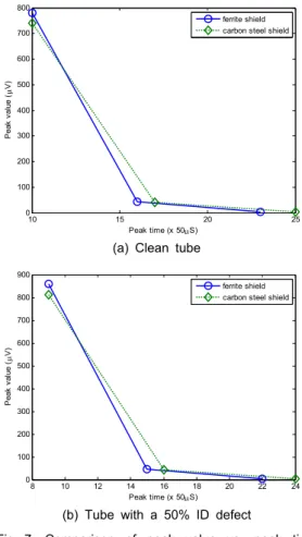
If shielding is used, the signal strength would be reduced. So, it is important to choose a proper and effective shielding material. In this work, ferrite shielding and carbon steel shielding were compared. Fig. 5 shows shielded sensor signals from a clean tube with ferrite and carbon steel shielding. The peak values versus corresponding peak times are drawn in Fig. 6 for both shielding cases. They show that the peak value of the signal reduces, as before, as the sensor is located farther away from the exciter; but, at this time, the appearance of the peak (that is, peak time) is delayed with the increased distance. Fig. 6 also shows that the defect signal has the bigger peak amplitude and the quicker peak time in both shielding cases.
8 10 12 14 16 18 20 22 24 0
100 200 300 400 500 600 700 800 900
Peak time (x 50μS)
Peak value
( μV)
No defect 50% ID defect
10 15 20 25
0 100 200 300 400 500 600 700 800
Peak time (x 50μS)
Peak value ( μV)
ferrite shield carbon steel shield
(a) Peak value vs. peak time (ferrite shielding) (a) Clean tube
8 10 12 14 16 18 20 22 24 26
0 100 200 300 400 500 600 700 800 900
Peak time (x 50μS)
Peak value ( μV)
No defect 50% ID defect
8 10 12 14 16 18 20 22 24
0 100 200 300 400 500 600 700 800 900
Peak time (x 50μS)
Peak value ( μV)
ferrite shield carbon steel shield
(b) Peak value vs. peak time (carbon steel shielding) (b) Tube with a 50% ID defect Fig. 6 Peak value vs. peak time from ferrite and
carbon steel shielding
Fig. 7 Comparison of peak value vs. peak time from ferrite and carbon steel shielding, without and with a defect
Fig. 7 compares the peak value versus peak time from both shielding cases, without and with a defect. It can be seen that the peak value from ferrite shielding is slightly bigger and the peak time appears quicker than those from the carbon steel shielding, whether there is a defect or not. Therefore, ferrite shielding was chosen for further study.
5. Sensitivity of Peak Value to Defect Size
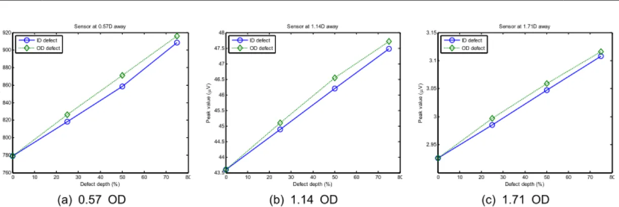
The sensitivity of peak value to defect depth variation was first investigated for both ID and OD defects and at three different sensor locations. The location of defect was just under the encircling exciter coil and its length was
6.35 mm. The depths were 25%, 50%, and 75%
of the wall thickness. The results are shown in Fig. 8. They show that the peak value increases as the defect depth increases regardless of sensor locations and OD defect signals have higher peak values than ID defect signals. The sensitivity of peak value to defect length variation was also investigated for both ID and OD defects and at three different sensor locations. The location of defect was just under the encircling exciter coil and its depth was 50% of the wall thickness. The lengths of defects were 2.54, 6.35, and 10.16 mm. The results are shown in Fig. 9. They show that the peak value increases as the defect length increases regardless of sensor locations and OD
0 10 20 30 40 50 60 70 80 760
780 800 820 840 860 880 900 920
Defect depth (%)
Peak value (
μV)
Sensor at 0.57D away ID defect
OD defect
0 10 20 30 40 50 60 70 80
43.5 44 44.5 45 45.5 46 46.5 47 47.5 48
Defect depth (%)
Peak value (
μV)
Sensor at 1.14D away ID defect
OD defect
0 10 20 30 40 50 60 70 80
2.95 3 3.05 3.1 3.15
Defect depth (%)
Peak value (
μV)
Sensor at 1.71D away ID defect
OD defect
(a) 0.57 OD (b) 1.14 OD (c) 1.71 OD
Fig. 8 Peak values from various ID and OD defect depths at three different sensor locations
0 2 4 6 8 10 12
760 780 800 820 840 860 880 900 920 940
Defect Length (mm)
Peak value ( μV)
Sensor at 0.57D away ID defect
OD defect
0 2 4 6 8 10 12
43.5 44 44.5 45 45.5 46 46.5 47 47.5 48 48.5
Defect Length (mm)
Peak value
( μ
V)
Sensor at 1.14D away ID defect
OD defect
0 2 4 6 8 10 12
2.95 3 3.05 3.1 3.15
Defect Length (mm)
Peak value
( μ
V)
Sensor at 1.71D away ID defect
OD defect
(a) 0.57 OD (b) 1.14 OD (c) 1.71 OD
Fig. 9 Peak values from various ID and OD defect lengths at three different sensor locations
0 10 20 30 40 50 60 70 80
1 1.02 1.04 1.06 1.08 1.1 1.12 1.14 1.16 1.18
Defect depth (%)
Normalized peak value
ID defect at 0.57D ID defect at 1.24D ID defect at 1.71D OD defect at 0.57D OD defect at 1.24D OD defect at 1.71D
0 2 4 6 8 10 12
1 1.02 1.04 1.06 1.08 1.1 1.12 1.14 1.16 1.18 1.2
Defect Length (mm)
Normalized peak value
ID defect at 0.57D ID defect at 1.24D ID defect at 1.71D OD defect at 0.57D OD defect at 1.24D OD defect at 1.71D
Fig. 10 Normalized sensitivity of peak value to ID and OD defect depth variation in an aluminum tube
Fig. 11 Normalized sensitivity of peak value to ID and OD defect length variation in an aluminum tube
defect signals have higher peak values than ID defect signals.
In order to decide a proper sensor location, the peak value sensitivity to defect size variation from various sensor locations needs to be compared. For this purpose, all the peak values were normalized by the peak values obtained when no defect was present at the respective sensor locations. The normalized sensitivity of
peak value to defect depth variation and to defect length variation in an aluminum tube are compared in Fig. 10 and 11, respectively. It can be seen that the peak value is more sensitive to defect size variation when the sensor is located closer to the exciter coil. In addition, the bigger difference between ID and OD normalized peak values can be noticed as the sensor is located closer to the exciter.
6. Conclusion
Based on numerical analysis results, this paper proposes a shielded encircling send-receive type PEC probe for the inspection of aluminum tubes from the outside. When bare coils were used, the peak time of the sensor signal did not change, even though the distance between the exciter and the sensor increased. This is due to the direct influence of the exciter flux. Thus, the exciter and the sensor coils were shielded so as to avoid direct influence of the exciter flux.
Numerical simulation with the designed shielded encircling PEC probe showed the corresponding increase of the peak time as the distance between the exciter and the sensor increased.
Since the peak value got reduced due to the use of the shielding material, the effects of different shield materials were also studied. Ferrite and carbon steel shields were compared and it was found that the ferrite shielding resulted in a slightly greater peak value and a quicker peak time. It was also found that the peak value increased and the peak time appeared more quickly when a defect was present.
The sensitivity of peak value to defect size variation was also investigated and found that, regardless of sensor locations, the peak value increased as the defect size, such as depth and length, increased. OD defect signals had stronger peak values than ID defect signals. To decide a proper sensor location, all the peak values were normalized by the peak values of no defect signal at the respective sensor locations. The normalized peak value sensitivity to defect size variation was compared. Results show that the normalized peak value was more sensitive to
defect size variation when the sensor coil was located closer to the exciter. In addition, the bigger difference between ID and OD normalized peak values was noticeable as the sensor was located closer to the exciter. Such promising results have shown that the proposed probe could be used effectively in the inspection of aluminum tubes.
References
[1] J. Blitz, "Electrical and Magnetic Methods of Nondestructive Testing," Bristol: Adam Hilger (1991)
[2] C. J. Renken, "The use of a personal computer to extract information from pulsed eddy current," Materials Evaluation, Vol. 59, No. 3, pp. 356-360 (2001)
[3] Y. K. Shin and D. M. Choi, "Design of a shielded reflection type pulsed eddy current probe for the evaluation of thickness," Journal of the Korean Society for Nondestructive Testing, Vol. 27, No. 5, pp. 398-408 (2007)
[4] Y. K. Shin, D. M. Choi and H. S. Jung,
"Comparison of simulated PEC probe performance for detecting wall thickness reduction," Journal of the Korean Society for Nondestructive Testing, Vol. 29, No. 6, pp. 563-569 (2009)
[5] Y. K. Shin, D. M. Choi, Y. J. Kim and S. S. Lee, "Signal characteristics of differential pulsed eddy current sensors in the evaluation of plate thickness," NDT&E International, Vol. 42, No. 3, pp. 215-221 (2009)