A Low Close-in Phase Noise 2.4 GHz RF Hybrid Oscillator using a Frequency Multiplier
†Hyunwon Moon1)*
Abstract This paper proposes a 2.4 GHz RF oscillator with a very low close-in phase noise performance. This is composed of a low frequency crystal oscillator and three frequency multipliers such as two doubler (X2) and one tripler (X3). The proposed oscillator is implemented as a hybrid type circuit design using a discrete silicon bipolar transistor. The measurement results of the proposed oscillator structure show -115 dBc/Hz close-in phase noise at 10 kHz offset frequency, while only dissipating 5 mW from a 1-V supply. Its close-in phase noise level is very close to that of a low frequency crystal oscillator with little degradation of noise performance. The proposed structure which is consisted of a low frequency crystal oscillator and a frequency multiplier provides new method to implement a low power low close-in phase noise RF local oscillator.
Key Words : RF oscillator, crystal oscillator, Frequency multiplier, Close-in phase noise, Low power, RLC tank, Q-factor, Silicon bipolar transistor, Hybrid circuit
1. Introduction
In general, a local oscillator (LO) is indispensable used to provide the carrier signal for both transmitter and receiver. In most RF transceivers, one input of mixer, which is used for frequency translation of the wanted signals, is driven by a periodic signal from a LO block.
Therefore, the spectral purity of the LO signal is very important in the modern wireless communication systems because its phase noise gives rise to the reciprocal mixing problem and the
* Corresponding Auther : [email protected]
†This research was supported by the Daegu University Research Grant 2012.
Manuscript December 12, 2014 / Revised February 06, 2015 / Accepted February 09, 2015
1) Assistant Professor, School of Electronic and Electric Engineering/Information and Communication Research Center(ICRC), Daegu University, South Korea
unwanted interference signals in the transmitter [1]. Also, the phase noise of a LO signal will corrupt the information transmitted through the frequency or phase of the carrier. For example, when a QPSK modulation signal is down- converted by a noisy LO, the signal constellation will be deviated from its ideal point. Thus, the bit error rate (BER) in the receiver may increase significantly. Therefore, the previous works have been published to improve the phase noise performance of RF oscillator [2]-[4]. Most of the previous works concentrate on the techniques to reduce the noise of the intermediate offset frequency from the carrier.
But, part of wireless communication systems with a narrow channel spacing, such as Japanese personal digital cellular (PDC), Korean domestic standard at a 400∼500 MHz band, FM radio, and
wireless sensor network, requires low phase noise at a few kHz offset frequency. Although several techniques were presented to obtain very low close-in phase noise performance [5-6], their usefulness is almost limited because an improvement of close-in phase noise performance is very small. Also, the power consumption of LO is very high relative to other blocks of RF transceiver, such as LNA, Mixer, and etc., because the required negative-gm increases as the operation frequency of LO is higher. Therefore, it is necessary to implement an RF oscillator with low power low close-in phase noise performance.
In this paper, an efficient method to implement an RF oscillator with low close-in phase noise operating at 2.4 GHz ISM band is proposed. The proposed RF oscillator is used at RF transceiver for a wireless sensor network and its performance is verified. It shows very good phase noise characteristic. It is implemented as a hybrid circuit type using discrete devices.
2. Design of RF Oscillator using a Crystal Oscillator and Frequency Multiplier A crystal oscillator is widely used as a reference clock for most of electronic systems and it has very low phase noise performance due to high Q factor of quartz crystals ranging from 10000 to several hundred thousand. Usually, the GHz frequency signal is required for many RF transceivers and digital processors. However, the crystal oscillator can not directly apply to above electronic devices because the frequency range of crystal oscillator is several tens of MHz. To obtain a higher frequency clock signal for the high speed digital system and RF LO signal for the wireless communication system, a phase locked loop (PLL) or delay locked loop (DLL) with a crystal oscillator is generally used [7-8]. But, the drawbacks of these approaches are the additional
Fig. 1 Proposed RF oscillator structure
noise sources of other circuit blocks and high current consumption. Although the new technique using a DLL structure is recently reported to synthesize a RF LO signal which phase noise is closely related to that of the reference signal, it should require a very high current consumption [9]. Therefore, to overcome these problems and obtain very low close-in phase noise performance, we propose new RF oscillator structure as shown in Fig. 1. It is composed of a high frequency crystal oscillator and three frequency multipliers such as two frequency doublers and one frequency tripler. If an active frequency multiplier is carefully designed, it is possible to implement a low power RF oscillator with little phase noise degradation.
Also, it is very important to select the frequency of crystal oscillator and what kinds of frequency multipliers (X2 or X3) because of the occurrence unwanted harmonic components.
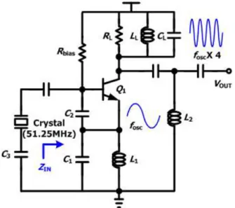
Figure 2 shows the schematic of a crystal oscillator. In general, it is impossible to directly realize the crystal oscillator operating a few hundreds of MHz resonance frequency because the practical frequency range for fundamental mode AT-cut crystals is 600 kHz to 30 MHz. To implement a 205 MHz crystal oscillator, we use a 52.25 MHz third overtones crystal and fourth-order frequency multiplier as shown in Fig. 2. We determine a Colpitts type oscillator structure because its output part will be separated from the oscillation region. So, the frequency quadruplet (X4) function can be easily implemented at output node of oscillator without an addition circuits and power consumption.
Fig. 2 Schematic of a 205 MHz crystal oscillator with 4th-order frequency multiplier
The real part and imaginary part of the input impedance (ZIN) of Fig. 2 as
(1)
║
(2)
The negative real part of ZIN is determined by the transconductance (gm) of Q1, C1 and C2. So, we choose the capacitance of C1 and C2 at the same value (C1=C2=C) for the maximum negative impedance to minimize the bias current. And the oscillation frequency is set by the equivalent inductance of the crystal and C. Also, L2 is added for preventing the unwanted fundamental oscillation caused by the third overtones crystal. And C3 is utilized for fine tuning of the oscillation frequency in the range of a few kHz. The RLC tank, composed of RL, LL, and CL, at the output node selects the fourth harmonic of the collector current of the crystal oscillator four times the fundamental frequency and it simply plays a role as a frequency multiplier.
First, we get the impulse response of RLC tank using a Laplace transform for optimizing the design value of each elements of a parallel RLC circuit as seen in Fig. 3(a).
(a) Equivalent circuit at the output load of the proposed crystal oscillator as shown in Fig.2
(b) Impulse response of a parallel RLC circuit
Fig. 3 Characteristics of frequency multiplier implemented by a RLC tank
cos
(3)
where
Also, Q-factor of RLC tank is defined as
(4)
If Q-factor is higher than 10, Equation (3) will be approximately as below
≈
(5)
So, we can know that from Equation (5) if a step function drives the tuned circuit, it caused to ring at its resonant frequency which is four times oscillation frequency. Since there is continuing supply of energy from the crystal oscillator, the signal generated from frequency multiplier can be maintained at output without ringing decays with time.
Fig. 4 Simulation result of the proposed crystal oscillator with a frequency multiplier
In General, the RLC tank with a high Q-factor has a good harmonic rejection. But, it is difficult to match the output impedance and is very sensitive to the parameter variations. It is very interesting that the output power of a frequency multiplier is inversely proportional to C as seen in Equation (5) and Fig. 3(b). Therefore, the Q-factor of RLC tank should be selected low to increase the output power for a maximum power efficiency.
However, if a matching circuit is additionally used, the Q-factor of a frequency multiplier is changed from low to high. It gives rise to decease the output power. To solve this problem, L2 is added to isolate between RLC tank and matching block as shown in Fig. 2. Also, the proposed crystal oscillator with a frequency multiplier of Fig. 2 operates as a class C type for generating the wanted harmonic frequency and a high power
efficiency.
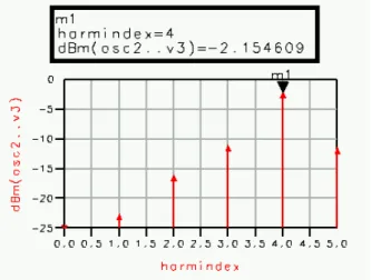
Figure 4 is the simulation result of the proposed 205 MHz crystal oscillator with frequency quadruplet (X4) function. The most largest harmonic component is the fourth harmonic frequency by virtue of a frequency multiplier. Its simulated output power level is about -2 dBm at 1-V power supply as seen in Fig. 4.
Figure 5 shows the circuit schematic of the
Fig. 5 Schematic of a frequency multiplier for doubler and tripler
Fig. 6 Simulated output spectrum of 2.46 GHz RF oscillator
frequency multiplier to implement RF LO from the proposed crystal oscillator. The main design point of the frequency multitier is power efficiency and harmonic rejection characteristics. So, it is very important to select a bias point and improve the
ability to reject an unwanted harmonic frequency.
To achieve these goals, the frequency multiplier is based at near pinch-off or forward region for creating an output current clipping. Also, the series resonance circuit consisted of L3 and C3 at output node is used for an unwanted harmonic termination. In particular, the 2nd harmonic termination at the input terminal should be well realized to minimize the effects by the feedback of harmonic components at output node. Similar to the crystal oscillator, the parallel RLC tank is used to select a wanted frequency component and low Q matching method is applied.
Blocks Output power
[dBm] Current [mA]
Crystal oscillator
(205 MHz) -5 0.6
Frequency Multiplier[X2]
(205 → 410) MHz -10 1.1
Frequency Multiplier[X3]
(410 → 1230) MHz -10 1.5
Frequency Multiplier[X2]
(1230 → 2460) MHz -10 1.8
Table 1 Output power and current consumption of each block of the proposed RF oscillator
Figure 6 is the simulated result of the proposed RF oscillator as shown in Fig. 1 using Agilent ADS circuit simulator. The final RF frequency is 2460 MHz after going through three frequency multipliers from a 205 MHz crystal oscillator. The output power level is about -7 dBm and the minimum harmonic rejection level is about 15 dB.
3. Measurement Results
The proposed 2.4 GHz band RF oscillator is implemented as a hybrid circuit type using a discrete silicon NPN BJT (Infineon BFP405). This silicon bipolar transistor is utilized for all circuits such as a crystal oscillator and three frequency
multipliers. Table 1 summarizes the measurement results of each block of the proposed 2.46 GHz hybrid RF oscillator. The total current consumption of all blocks is about 5 mA as shown in Table 1.
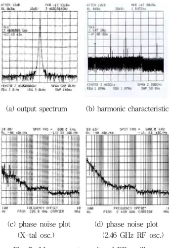
The final output power level of the proposed RF oscillator is measured about -10 dBm at 50-Ω impedance for supply voltage of 1-V as shown in Fig. 7 (a) and (b). Its frequency response is measured by HP8564E spectrum analyzer including a line loss. There exist various unwanted harmonic frequencies as seen in Fig. 7 (b). But, it doesn't
(a) output spectrum (b) harmonic characteristic
(c) phase noise plot (d) phase noise plot (X-tal osc.) (2.46 GHz RF osc.) Fig. 7 Measurement results of RF oscillator
matter because the power difference between the wanted signal and maximum harmonic frequency (2050 MHz) is above 20 dBc which value is enough large. Figure 7 (d) shows the phase noise performance of the proposed RF oscillator. The phase noise performance is very similar to that of
a crystal oscillator although its phase noise performance is slightly degraded compared with that of the crystal oscillator as seen in Fig. 7 (c).
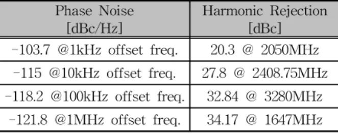
The measured phase noise is -115 dBc/Hz at 10 kHz offset frequency. This close-in phase noise value is very low as an RF oscillator with 2.46 GHz center frequency. The measurement results of the proposed oscillator about phase noise and harmonic rejection performance are summarized in Table 2.
To compare performance of the proposed oscillator with the previous published results, we define a normalized figure of merit (FOM) as below [3].
log
log
(6)Phase Noise
[dBc/Hz] Harmonic Rejection [dBc]
-103.7 @1kHz offset freq. 20.3 @ 2050MHz -115 @10kHz offset freq. 27.8 @ 2408.75MHz -118.2 @100kHz offset freq. 32.84 @ 3280MHz
-121.8 @1MHz offset freq. 34.17 @ 1647MHz Table 2 Measurement results of phase noise and
harmonic rejection performance
Technology Parameter This
work CMOS
[5] CMOS
[9] SiGe [10]
Freq. [GHz] 2.46 1.54 0.9 7.55 PN @ 30kHz
[dBc/Hz] -115 -100 -120 -115
Supply voltage 1V 2.7V 3.3V 3.3V
Current 5mA 6mA 39mA 14.2mA
Power
consumption 5mW 16.2mW 130mW 47mW FOM [dBc/Hz] -206.3 -182.1 -188.4 -206.3 Table 3 Measurement results of the proposed
oscillator compared with the previous works
Table 3 shows the results compared the proposed oscillator with the previous studies. As we can know from Table 3, the normalized FOM of the propose RF oscillator structure is superior or similar to the previous works about the close-in phase noise performance.
4. Conclusion
In this paper, a high frequency oscillator that has a low power consumption and low close-in phase noise performance is realized using a crystal oscillator and three frequency multipliers. The proposed RF local oscillator shows a very low close-in phase noise of -115 dBc/Hz that is similar to that of a crystal oscillator consuming only 5 mA current at supply voltage of 1V. Also, to meet the wanted output power level and harmonic rejection performance, various techniques such as low Q matching network, the harmonic termination, and harmonic rejection, are applied. The proposed structure is very efficient method to implement a very low close-in phase noise RF oscillator.
References
[1] B. Razavi, "RF Microelectronics", Upper Saddle River, NJ, Prentice-Hall, 1998.
[2] A. Hajimiri and T. H. Lee, "Design issues in CMOS differential LC oscillators" IEEE J.
Solid-State Circuits, Vol. 34, No. 5, pp.717-724, 1998.
[3] E. Hegazi, H. Sjöland, and A. A. Abidi, "A filtering technique to lower LC oscillator phase noise," IEEE J. Solid-State Circuits, Vol. 36, No. 12, pp.1921-1930, 2001.
[4] Z. Li and K. K. O, "A low-phase noise and low-power multiband CMOS voltage controlled oscillator," IEEE J. Solid-State Circuits, Vol.
40, No. 6, pp.1296-1302, 2005.
[5] A. Ismail and A. A. Abidi, "CMOS differential LC oscillator with suppressed up-converted flicker noise," February 9-13, 2003, San Francisco, CA, USA, pp. 98-99 in IEEE ISSCC Digest.
[6] H. Moon and I. Nam, "1.3 V low close-in phase noise NMOS LC-VCO with parallel PMOS transistors," IET Electronics Letters, Vol. 44, No. 11 pp.676-678, 2008.
[7] J. Craninckx and M. Steyaert, "Wireless CMOS frequency synthesizer design", Boston, Kluwer Academic Publishers, 1998.
[8] H. P. Kim and I. C. Hwang, "A low-power, low-noise DLL-based frequency multiplier for reference clock generator," Journal of the Korea Industrial Information System Research, Vol.
18, No. 5, pp. 9-14, 2013.
[9] G. Ghien and P. R. Gray, "A 900MHz local oscillator using a DLL-based frequency multiplier technique for PCS applications," February 6-10, 2000, San Francisco, CA, USA, pp. 202-203 in IEEE ISSCC Digest.
[10] A. Esswein, G. Dehm-Andone, R. Weigel, A.
Aleksieieva, and M. Vossiek, "A low phase- noise SiGe colpitts VCO with wide tuning range for UWB applications," September 28-30, 2010, Paris, France, pp. 1599-1602 in Proc.
EuMC.
문 현 원 (Hyunwon Moon)
∙정회원
∙1997년 2월 한양대학교 전파공학 과 공학사
∙1999년 2월 한국과학기술원 전기 및 전자공학과 공학석사
∙2004년 8월 한국과학기술원 전기 및 전자공학과 공학박사
∙2004년 7월 ∼ 2012년 2월 삼성전자 SYSTEM LSI 사업부 책임연구원
∙2012년 3월 ∼ 현재 대구대학교 정보통신대학 전 자전기공학부 조교수
∙관심분야 : Analog/RF circuit design, PMIC design, Sensor Interface circuit design