Vol. 21, No. 12 (2011)
703
†Corresponding author
E-Mail : [email protected] (Y. -C. Nah)
Effects of Sputter Parameters on Electrochromic Properties of Tungsten Oxide Thin Films Grown by RF Sputtering
Yoon-Chae Nah
†School of Energy·Materials·Chemical Engineering, Korea University of Technology and Education, Cheonan 330-708, Korea
(Received October 31, 2011 : Received in revised form November 23, 2011 : Accepted December 5, 2011)
Abstract
The electrochromic properties of tungsten oxide films grown by RF sputtering were investigated. Among the sputter parameters, first the Ar:O2 ratios were controlled with division into only an O2 environment, 1:1 and 4:1. The structure of each film prepared by these conditions was studied by X-ray diffraction, X-ray photoelectron spectroscopy and Rutherford backscattering spectroscopy. The sputter-deposited tungsten oxide films had an amorphous structure regardless of the Ar:O2 ratios. The chemical compositions, however, were different from each other. The stoichiometric structure and low-density film was obtained at higher O2 contents. Electrochemical tests were performed by cyclic voltammetry and chronoamperometry at 0.05 M H2SO4 solutions. The current density and charge ratio was estimated during the continuous potential and pulse potential cycling at −0.5 V and 1.8 V, respectively. The film grown in a higher oxygen environment had a higher current density and a reversible charge reaction during intercalation and deintercalation. The in-situ transmittance tests were performed by He-Ne laser (633 nm). At higher oxygen contents, a big transmittance difference was observed but the response speed was too slow.This was likely caused by higher film resistivity. Furthermore, the effect of sputtering pressure was also investigated. The structure and surface morphology of each film was observed by X-ray diffraction and scanning electron microscopy. A rough surface was observed at higher sputtering pressure, and this affected the higher transmittance difference and coloration efficiency.
Key words
tungsten oxide, RF sputtering, electrochromism.1. Introduction
Electrochromic phenomena can be observed for a range of transition metal oxides and are based on a reversible change in colors during electrochemical oxidation/reduc- tion processes.
1-3)The electrochromic behavior can be ex- plained by a combinational injection and extraction of electrons and ions. During an electrochromic process, at a given voltage, electrons are injected (reduction) or extract- ed (oxidation) and, at the same time, ions are moved into or out of the electrochromic materials to balance charge neutrality.
Tungsten oxides (WO
3) have been extensively studied as electrochromic materials because they exhibit a high coloration efficiency and a high cyclic stability compared to other transition metal oxides. These features provide the basis for their applications in smart windows, reflectance variable mirrors, and information displays.
4-6)It is widely accepted that the electrochromic phenomenon of WO
3is due to the formation of tungsten bronze (M
xWO
3) according to the following equation:
WO
3+ xe
−+ xM
+↔M
xWO
3(1)
with M
+= H
+, Li
+, Na
+, K
+, and e- denoting electrons.
When electrons and ions are injected, the electronic struc- ture of WO
3is modified. The Fermi level is moved upward, and excess electrons fill the t
2gband of WO
3.
7)This strongly alters the optical properties of the material from transparent to a deep blue color.
Tungsten oxide films can be prepared by several methods such as evaporation, sputtering, electrodeposition and sol- gel process.
8-11)Sputtering method, among them, is a well- established technique for thin film preparation. Sputter par- ameters, which include such as Ar:O
2ratios, sputtering pressure and RF power can be important factors to deter- mine electrochromic properties of tungsten oxide, because electronic or structural states of tungsten oxide film are directly related to electrochromic properties.
Therefore, in this work, the electrochromic properties of sputter-deposited tungsten oxide film were investigated with various conditions of Ar:O
2ratios and sputtering pressure in H
2SO
4solutions. The relationships between electronic or structural states and electrochromic properties of tungsten oxide were examined.
2. Experimental Procedure
Tungsten oxide films were grown by using an RF mag-
netron sputtering system. ITO (Samsung Corning Co, Ltd.) coated transparent glass was used as the substrate. The thickness and resistivity of the ITO was about 800 Å and 50 Ω/square. WO
xused as the target material and the distance between the target and the substrate was 8 cm. The base pressure was below 5 × 10
−6Torr. Prior to sputtering, a pre-sputtering process was performed for 10 minutes to eliminate contamination from the target. Two conditions were controlled in sequence during the sputtering; Ar:O
2ratios and sputtering pressure.
In order to investigate the effect of gas composition, the ratios of Ar:O
2were controlled; only O
2, 1:1 and 4:1. The sputtering pressure and RF power were sustained during the sputtering at 5 mTorr and 60 W, respectively. The films thickness of all the tungsten oxide films were carefully measured by cross-sectional scanning electron microscopy (SEM, D/Max-2400, Rigaku) and the film density was calculated using Rutherford backscattering spectroscopy (RBS, 3SDH, NEC) data. The thickness of the films prepared here were 200, 190 and 200 nm for only O
2, 1:1 and 4:1, respectively. A dose of 10 µC of He
++ions was used to obtain RBS spectra. The ions had an incident energy of 2.24 MeV and a scattering angle of 165
o. Hypra, Charls Evans & Associates’ simulation software program, was used for the analysis of RBS data. Crystallographic structure was measured by X-ray diffraction measure- ments, using a Rigaku diffractometer operated with a Cu K
αradiation source at 40 kV and 40 mA.
The sputtering pressure was controlled in 5 mTorr, 10 mTorr and 20 mTorr at the condition of constant sputtering gas (only O
2) and RF power (60 W). The crystallographic structure and surface morphology were measured by the X- ray diffraction and scanning electron microscopy.
All the electrochemical tests were performed using an Autolab PGSTAT30 Potentiostat/Galvanostat (Netherlands).
Tungsten oxide films were used as the working electrode.
Pt and Ag/AgCl (sat. KCl) were used as the counter and reference electrodes, respectively. The electrolyte was 0.05 M H
2SO
4solution and measured pH was about 1.9.
Continuous potential cycling was carried out for up to 50 cycles in the range of –0.5 V to 1.8 V at a scan rate of 10 mV/s. The electrochromic response time was then tested by applying a pulse potential between –0.5 V and 1.8 V with a duration time of 30 seconds. The optical transmit- tance was simultaneously measured in situ during all the experiments by using a He-Ne laser (633 nm, 10 mW).
The transmittance of the ITO/glass with the electrolyte and the cell window was assumed to be 100 %.
3. Results and Discussion
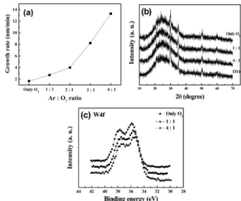
Fig. 1(a) shows growth rates of tungsten oxide films as a function of Ar:O
2ratios. The growth rate decreases as
the contents of oxygen increases, because the tungsten target is easily oxidized in the oxygen ambient, so that sputter yield is decreased. The crystallographic structures of tungsten oxide films grown by different Ar:O
2ratios are illustrated in Fig. 1(b). The pure ITO substrate shows a broad peak derived from the glass substrate at low angle and small sharp peaks at 2 θ = 30.1
o, 35.2
o, 50.5
oand 59.9
o. A distinct feature of tungsten oxide film is not observed with a broad peak because all the films have amorphous structure regardless of different Ar:O
2ratios.
However, the chemical composition is depending on the ratios. Fig. 1(c) shows W4f XPS data for these films. It is reasonable that the binding energy of W4f shift to lower at the decrease of oxygen contents because of screening effect. This means that the oxidation state of tungsten oxide becomes far from stoichiometric structure. It is clearly confirmed that the binding energy of W4f
2/7peaks is lower shifted from 35.79 eV to 35.38 eV as the oxygen contents is decreased. Meanwhile, considering that the bind- ing energy in case of WO
2is 34.3 eV,
12)sputtered tungsten oxide films have a sub-stoichiometric phase (WO
x) with some edge sharing octahedral. This edge sharing may lead an increase of film density which is verified from RBS data that the film deposited at lower oxygen contents have a large film density; 8.08 × 10
22atoms/cm
3and 8.37 × 10
22atoms/cm
3for only O
2and 4:1, respectively. The electro- chemical tests are affected by the film density.
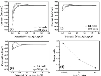
Fig. 2(a) shows a cyclic-voltammetry (CV) of the films in the range of −0.5 V-1.8 V. It is easy to understand that a large CV curve is obtained in the case of only O
2(Fig. 2(a)) and small amounts of current is incorporated in the Fig.
2(b) and (c) which show a slight difference. This means
Fig. 1. (a) Growth rate of tungsten oxide films as a function of Ar:O2 ratios, (b) X-ray diffraction patterns for ITO substrate and each film prepared at different Ar:O2 ratios and (c) X-ray photoelectron spectra of W4f for each film prepared at different Ar:O2 ratios.
that a low film density make protons enough to permeate into the films. Fig. 2(d) shows a charge ratio, which value is to divide deintercalated charge by intercalated charge. It is interesting to know that the charge ratio is increased as the oxygen contents are increased. In other words, the intercalated charges under the cathodic potential are almost extracted (or deintercalated) under reverse potential in the case of only O
2. However, the deintercalated charge is much less than intercalated charge, which consequently shows a small charge ratio. It means that a reversible reaction occurs when oxygen contents are large and then film density is low enough for protons to permeate into the film.
Fig. 3 shows the in-situ transmittance test during the potential cycling for each sample. It can be instantly recognized that the film prepared at only O
2ambient shows a stable electrochromic performance, not in the 1:1 or 4:1 conditions, which have a fluctuation in transmittance.
This may be why stoichiometric WO
3film is more stable in the region of cycling voltage in acid electrolyte. Besides, the transmittance difference in the Fig. 3(a) is higher than in the Fig. 3(c) with the same film thickness (200 nm). It is attributed to more open structure at only O
2ambient. It is to be sure that a stable electrochromic performance can be shown from Fig. 3(a) in which transmittance at minimum colored state and maximum bleached states for 50th cycle is larger than that for 1st cycle. In the condition of 1:1 (Fig.
3(b)), the minimum colored state is only lowered and the maximum bleached state is maintained for the entire cycling. However, in the condition of 4:1 (Fig. 3(c)), the minimum bleached state at 50th cycle is lowered compared to at 1st cycle. It means that intercalated protons remain
without a complete extraction at reverse potential, so that small amount of color is stored in the film which is a factor of irreversibility and degradation.
13,14)Fig. 4(a) shows a response time for each film. The response time is regarded as the time to reach 80% of maximum transmittance change. From the Fig. 4(a), it is appreciated that the response time is faster at lower oxygen contents. This does not provide a full understanding because protons are more permeable at stoichiometric structure. Meanwhile, He et al. reported that the response time is decreased with increasing O
2/Ar flow ratio due to the corner sharing structure (open structure).
15)In this report, however, it is suggested that the response time is more influenced on the film resistivity. Fig. 4(b) shows the film resistivity measured by 4-point probe method for each sample. The film resistivity is decreased with decreas- ing oxygen contents. It may lead a faster response time.
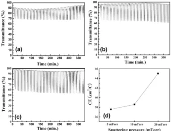
In order to investigate the effect of sputtering pressure on electrochromic properties, three different gas pressures were employed; 5, 10, 20 mTorr. It is confirmed that films are slowly deposited at higher pressure, which is because sputtered tungsten atoms are scattered by gas molecules before deposition and therefore mean free path of the
Fig. 3. In-situ transmittances during the potential cycling for each film prepared at different Ar:O2 ratios; (a) only O2, (b) 1:1 and (c) 4:1.Fig. 4. (a) Response time during the coloring and bleaching process and (b) film resistivity measured by 4-point probe method for each film prepared at different Ar:O2 ratios.
Fig. 2. Cyclic voltammograms of each tungsten oxide film prepared at different Ar:O2 ratios; (a) Only O2, (b) 1:1 and (c) 4:1. The dashed and solid lines represent the 1st and the 50th cycle during the potential cycling, respectively. (d) charge ratio (deintercalated charge density / intercalated charge density) which is calculated from chronoamperometry curves.
atoms are shorten. By XRD results, deposited films have all amorphous structures regardless of sputtering pressure (not shown here). In the SEM images (Fig. 5), however, there is a significant difference in surface morphology.
Fig. 5(a) shows very smooth and homogeneous surface compared to others. On the other hand, the tungsten oxide film grown at a high working pressure appeared to have a large-grain and rough surface morphology shown in the Fig. 5(b) and (c). This can be explained that a slow growth rate at higher working pressure conditions provide sufficient time for adatoms to partially get together, so that consequently produces high grain and rough surface.
The surface morphology of the films has influenced on the electrochromic performances. Fig. 6(a)-(c) shows an
in-situ transmittance for each film. The transmittance difference at 50th cycle is about 28.16% at (a) 5 mTorr, 34.67% at (b) 10 mTorr and 43.99% at (c) 20 mTorr. It is apparent that transmittance difference is larger at higher sputtering pressure. This can be explained as a relation- ship with surface morphology. The rougher surface may provide a more porous film structure and consequently protons can easily move into the films along the void networking. The increase of proton capacity leads finally a big transmittance difference. Fig. 6(d) shows a color- ation efficiency (CE) at different sputtering pressures. A higher CE is obtained at higher sputtering pressure. The exact mechanism with respect to CE is not clear yet,
16)but the increase of CE value at higher sputtering pressure may be also related to the rough surface and charge movement.
4. Conclusion
Effects of Ar:O
2ratios on the structure of tungsten oxide films, electrochemical and electrochromic properties were investigated. From XPS analysis, it is apparent that sputter- deposited film has a stoichiometric phase with corner sharing octahedra at higher oxygen contents. This could provide a lower film density, so that open-structured film was thought to be obtained compared to films which have lower oxygen contents. In the electrochemical test, a large amount of current density was produced at higher oxygen contents during the potential cycling. This could explain that a low film density caused by open structure make protons enough to intercalate or deintercalate in the film.
Meanwhile, a reversible reaction was occurred during the pulse potential, which is also resulted from open structure.
A larger transmittance difference was also obtained at higher oxygen contents attributed to higher current density. How- ever, response time was so slow because of higher film resistivity.
The structure and electrochromic properties of tungsten oxide film were also affected by sputtering pressure. A rough and non-homogeneous surface was obtained at higher sputtering pressure due to the slow growth rate that can lead for adatoms to partially get together. The higher surface roughness produced a big transmittance difference because the film might have a large porosity, so that proton can easily move into the film. An increase of coloration efficiency (CE) at higher sputtering pressure was obtained and this may be related to rough surface.
Acknowledgment
This paper was supported by research subsidy for newly- appointed professor of Korea University of Technology and Education for year 2011.
Fig. 5. SEM images for each film prepared at different sputtering pressures; (a) 5 mTorr, (b) 10 mTorr and (c) 20 mTorr.
Fig. 6. In-situ transmittances during the potential cycling for each film prepared at different sputtering pressures; (a) 5 mTorr, (b) 10 mTorr and (c) 20 mTorr and (d) Coloration efficiency (CE) calculated from charge density and optical density change (∆OD) at different sputtering pressures.
References
1. S. K. Deb, Phil. Mag., 27, 801 (1973).
2. P. M. S. Monk, R. J. Mortimer and D. R. Rosseinsky, Electrochromism: Fundamentals and Applications, p. 3, VCH, Weinheim (1995).
3. C. G. Granqvist, Handbook of Inorganic Electrochromic Materials, p. 1, Elsevier, Amsterdam, (1995).
4. S. -H. Lee, W. Gao, C. E. Tracy, H. M. Branz, D. K.
Benson and S. Deb, J. Electrochem. Soc., 145, 3545 (1998).
5. T. J. Richardson, J. L. Slack, R. D. Armitage, R. Kostecki, B. Farangis and M. D. Rubin, Appl. Phys. Lett., 78, 3047 (2001).
6. R. J. Mortimer, A. L. Dyer and J. R. Reynolds, Displays, 27, 2 (2006).
7. K. -W. Park, H. -S. Shim, T. -Y. Seong and Y. -E. Sung, Appl. Phys. Lett., 88, 211107 (2006).
8. I. Porqueras, G. Viera, J. Marti and E. Bertran, Thin Solid Films, 343-344, 179 (1999).
9. H. S. Withan, P. Chindaudom, I. An. R. W. Collins, R.
Messier and K. Vedam, J. Vac. Sci. Tech. A, 11(4), 1881 (1993).
10. A. Meulenkamp, J. Electrochem. Soc., 144, 1664 (1997).
11. T. C. Arnoldussen, J. Electrochem. Soc., 128, 117 (1981).
12. J. F. Moulder, W. F. Stickle, P. E. Sobol and K. D. Bomben, Handbook of X-ray Photoelectron Spectroscopy, p. 146-147 ed. J. Chastain and R. C. King, Jr., Physical Electronics, Minnesota, USA (1995).
13. J. Nagai, T. Kamimori and M. Mizuhashi, Proc. Soc.
Photo Opt. Instrum. Eng., 562, 39 (1985)
14. P. Falaras, A. Hugot-Le Goff and S. Joiret, Large-area Chromogenics: Materials and Devices for Transmittance Control, p. 16, ed. C. Lampert and C. Granqvist, SPIE Opt. Bellingham (1990)
15. J. L. He and M. C. Chiu, Surf. Coating. Tech., 127, 43 (2000).
16. S. H. Lee, H. M. Cheong, C. E. Tracy, A. Mascarenhas, A. W. Czanderna and S. K. Deb, Appl. Phys. Lett., 75, 1541 (1999).