Vol.18, No.4, (2016), pp.15~20 http://dx.doi.org/10.9714/psac.2016.18.4.015
```
1. INTRODUCTION
A high-temperature YBa 2 Cu 3 O 7-y (YBCO) superconductor is a promising material for practical applications because of the high superconducting critical temperature (T c ) of 91 K and high critical current density (J c ) in magnetic fields [1, 2]. For the practical use the YBCO superconductor in high magnetic fields, however, the value of J c should be increased further.
The J c of the YBCO superconductor is a function of the microstructure developed in the interior of the superconducting grains. Defects such as vacancy, dislocation, twins, stacking faults and non-superconducting lattice are developed during processing and oxygenation heat treatment [3-8]. They can effectively act as flux pinning sites which pin the flux in the superconducting matrix. When the defects are finely dispersed in the superconducting matrix, the value of J c in a high magnetic field can be increased.
The flux pinning center (nano-defects) can be produced through either a chemical method (impurity doping) or a physical method (irradiation). Chemical doping of impurity atoms to the superconductors can increase the flux pinning c a p a b i l i t y o f s u p e r c o n d u c t i n g p h a s e [ 9 ] . T h e addition of a second particle phase such as Y 2 BaCuO 5 to the melt processed YBCO superconductors also increase J c
in magnetic fields [10]. The superconductor/inclusion interfaces seems to trap the magnetic flux effectively.
On the other hand, particles such protons [11, 12], neutrons [13, 14], electrons [15, 16] and ions [17, 18] can be used as source particles for making defects in a superconducting matrix. High-energy irradiation can produce various defects (from a point defect to an extended columnar defect) in a superconductor matrix. The type of defect formed is dependent on the energy level of the accelerated particles [19].
In this study electron beam (EB) irradiation was attempted to generate defects in YBCO films with an aim of the enhancement of J c . The formation aspect of defects by EB irradiation and the influence of the formed defects on the superconducting properties of the YBCO films are reported.
2. EXPERIMENTAL PROCEDURE
The YBCO films used in this study were a commercial product of CERACO, Inc. (Germany) with dimensions of 10 mm × 10 mm. The films were grown on an Al 2 O 3 single crystal with a CeO 2 buffer. The thickness of the YBCO films was about 300 nm. To make specimens for EB irradiation, the YBCO films were cut into five pieces using a diamond cutter. Irradiation was carried out using a
Effects of electron beam irradiation on the superconducting properties of YBCO thin films
Y. J. Lee
a,b, J. H. Choi
a, B.-H. Jun
a, J. Joo
b, C. S. Kim
c, and C.-J. Kim
*,aa Korea Atomic Energy Research Institute, Daejeon, Korea
b Sungkyunkwan University, Suwon, Korea
c Korea Research Institute of Standards and Science, Daejeon, Korea
(Received 2 November 2016; revised or reviewed 12 December 2016; accepted 13 December 2016)
Abstract
The effects of electron beam (EB) irradiation on the superconducting critical temperature (T c ) and critical current density (J c ) of YBCO films were studied. The YBCO thin films were irradiated using a KAERI EB accelerator with an energy of 0.2 MeV and a dose of 10 15 –10 16 e/cm 2 . A small T c decrease and a broad superconducting transition were observed as the EB dose increased. The value of J c s (at 20 K, 50 K and 70 K) increased at doses of 7.5×10 15 and 2.2×10 16 e/cm 2 . However, J c s decreased as the dose increased further. The X-ray diffraction (XRD) analysis showed that the c axis of YBCO was elongated and the full width at half maximum (FWHM) increased as the dose increased, which is strong evidence of the atomic displacement by EB irradiation. The transmission electron microscopy (TEM) showed that the amorphous layer formed in the vicinity of the surfaces of the irradiated films. The amorphous phase was often present as an isolated form in the interior of the films. In addition to the formation of the amorphous phase, many striations running along the a-b direction of YBCO were observed. The high magnification lattice image showed that the striations were stacking faults. The enhancement of J c by EB irradiation is likely to be due to the lattice distortion and the formation of defects such as vacancies and stacking faults. The decrease in J c at a high EB dose is attributed to the extension of the amorphous region of a non-superconducting phase.
Keywords: YBCO, Critical current density(J
c), Electron beam irradiation, Defect, Flux pinning
* Corresponding author: [email protected]
Fig. 1. KAERI electron beam accelerator.
KAERI electron beam (EB) accelerator with an acceleration energy of 0.2 MeV and 1 mA (Fig. 1). At a constant energy of 0.2 MeV, the irradiation time was changed from 0 to 10 min. The irradiation doses calculated using equation (1) for the irradiation times of 0, 1, 3, 7, 10 min were 0, 7.5×10 15 , 2.2×10 16 , 5.2×10 16 and 7.5×10 16 e/cm 2 , respectively.
10
196 .
1
-
window of Area
T
Dose I (1)
The lattice parameter and full width at half maximum (FWHM) of YBCO films before/after irradiation were estimated using X-ray diffraction (XRD), scanned for 2θ at 20° – 80°. The lattice distortion by EB irradiation was estimated from the FWHM using a high-resolution XRD (HR XRD).
The superconducting properties were measured using a magnetic property measurement system (MPMS). The T c of the YBCO films, non-irradiated and irradiated at various EB doses, was estimated from the temperature-magnetic moment curves. To understand the effect of EB irradiation on J
c, magnetic moment-magnetic field curves at 20 K, 50 K and 70 K were measured for the irradiated films. The values of J c of the YBCO films were calculated using Bean’s critical model [20] of equation (2).
b) a/
a(
/ M
J
c 20Δ 1 3 (2)
Where ΔM is the magnetization difference (M_decreasing field region-M_increasing field region) in a constant magnetic field, and a and b are parameters regarding the sample dimensions.
The microstructures of the non-irradiated and irradiated films were investigated using transmission electron microscopy (TEM). The YBCO films were cut normal to the film surface using a focused ion beam (FIB).
The defects formed in the vicinity of the films surface and the interior of the films were investigated. The lattice images of the irradiated films were examined using a high resolution (HR) TEM.
3. RESULTS AND DISCUSSION
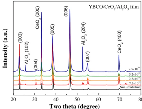
Fig. 2 shows the XRD patterns of the non-irradiated YBCO and irradiated films at various doses. The (102) and (204) peaks of the Al 2 O 3 substrate at 2θ=27° and 2θ=52°, the peak of the CeO 2 buffer layer and the (00l) peaks of YBCO films were observed in the XRD pattern. It can be recognized from the XRD patterns that the YBCO films are well aligned normal to the c-axis. A more precise analysis for the 2θ angle of the (006) peaks of the XRD patterns show that the (006) peak shifts to the low angle as the dose of EB irradiation increases (see Fig. 3), which indicates the change of the c parameter of YBCO [21].
The length of parameter c of each film was calculated using Bragg’s law of nλ=2dsinθ for the orthorhombic crystal structure, where λ is the wavelength of the target used, d is an inter-planar spacing, and θ is a Bragg diffraction angle. Fig. 4 shows that parameter c increases as the EB dose increases. Parameter c of the non-irradiated film was 11.635 Å and increased to 11.684 Å and 11.7036 Å as the EB dose increased to 2.2×10 16 e/cm 2 and 7.5×10 16 e/cm 2 , respectively. Parameter c of the YBa 2 Cu 3 O 7-y was known to be a function of oxygen content in the orthorhombic crystal structure [22]. The high-temperature tetragonal phase with lower oxygen content had a c parameter longer than the orthorhombic phase with higher
20 30 40 50 60 70 80
5.21016 7.51015 Non-irradiation 7.51016 2.21016
YBCO/CeO
2/Al
2O
3film
In te n si ty (a.u .)
Two theta (degree)
(003) Al2O3 (102) (004)CeO2 (200) (005) (006) Al2O3 (204) (007) CeO2 (400)
Fig. 2. XRD patterns of YBCO films, non-irradiated and irradiated at various EB doses.
46 47 48
7.51015 Non-irradiation 7.51016 5.21016 2.21016
YBCO/CeO
2/Al
2O
3film
In te n si ty (a.u .)
Two theta (degree) (006)
Fig. 3. Shift of 2θ of a (006) peak with EB dose.
oxygen content [23]. Even in the orthorhombic phase, the presence of more oxygen atoms in the crystal lattice shorten parameter c by the ordering of oxygen atoms in the 1 dimensional Cu-O chains located between two Ba-O layers [24, 25]. It indicates that some of the oxygen atoms are out of their own positions in the orthorhombic lattices from the EB irradiation.
The effects of EB irradiation on the crystallinity of YBCO films was analyzed using HR-XRD for the (006) peak appearing at 2θ = 46°. The FWHM data obtained from the ω scan rocking curve for the (006) peak are shown in Table Ι. The FWHM of the non-irradiated sample is 0.5491 and increased gradually as the EB dose increased. At an EB dose of 7.5×10 16 e/cm 2 , the FWHM is 0.8053. The increased FWHM with increasing EB dose indicates that the lattice displacement in YBCO films increased with an increase in EB dose.
Fig. 5 shows the magnetic moment-temperature curves of the YBCO films, non-irradiated and irradiated at various EB doses. The value of T c of the non-irradiated film is 84.5 K. The value of T c decreases to 81.5 K as the EB dose increased to 7.5×10 16 e/cm 2 . It should be noted that the variation in superconducting transition width (ΔT c ) owing to the EB irradiation is remarkable. The value of ΔT c is as large as 30-40 K at high EB doses. It can be generally expected that the superconducting transition is sharp and ΔT c is small when the superconducting phase is uniform [26]. The T c decrease and broadening of the superconducting transition by EB irradiation are strong e vi d e nc e o f t he s t r uc t ural damages by electron bombardment the change in superconducting critical
0.0 2.0x10
164.0x10
166.0x10
168.0x10
1611.62
11.64 11.66 11.68 11.70 11.72
C ( Å )
Dose (e/cm
2)
Fig. 4. The variation of parameter c with an EB dose.
TABLE Ι
F ULL WIDTH AT HALF MAXIMUM (FWHM) OF THE (006) PEAK AS A FUNCTION OF EB DOSE .
Dose(e/cm 2 ) FWHM(degree)
Non-irradiation 0.5491
7.5×10 15 0.5848
2.2×10 16 0.5878
5.2×10 16 0.6227
7.5×10 16 0.8053
20 40 60 80 100
-1.2 -0.8 -0.4
0.0 Non-irradiation 7.510
152.210
165.210
167.510
16c//H
Nor m ali ze d m agn et ic m om en t ( a.u .)
Temperature (K)
Fig. 5. The magnetic moment-temperature curves of the non-irradiated and irradiated YBCO films at various doses.
temperature agrees with the disordered lattices, and the c parameter change confirmed by through the XRD analysis in Figs. 3 and 4.
Fig. 6 shows the J c – B curves at (a) 20 K, (b) 50 K and (c) 70 K of the YBCO films non-irradiated and irradiated at various EB doses. As shown in Fig. 6(a), the value of J c at 20 K and 1 T and 3 T of the non-irradiated film is 1.54×10 6 A/cm 2 and 9.38×10 5 A/cm 2 , respectively. As the EB dose increases to 7.5×10 15 e/cm 2 and 2.2×10 16 e/cm 2 , the value of J c s at 1 T and 3 T increases to 5.77×10 6 , 3.59×10 6 A/cm 2 and 6.52×10 6 , 4.01×10 6 A/cm 2 , respectively. However, J c decreases as the EB dose further increases. The increase in J c at a specific level of EB dose indicates that there exists an optimum level of lattice disorder and defects. An enhancement of J
cthrough EB irradiation was also observed at 50 K and 70 K. At the same dose levels as shown in Fig.
6(a), J c s increases (see Figs. 6(b) and 6(c)). This result indicates that the defects formed by the EB irradiation act as effective flux pinning centers within a temperature ranges of 20 K – 70 K. The prolonged EB irradiation over 2.2×10 16 e/cm 2 also leads to a decrease in J c .
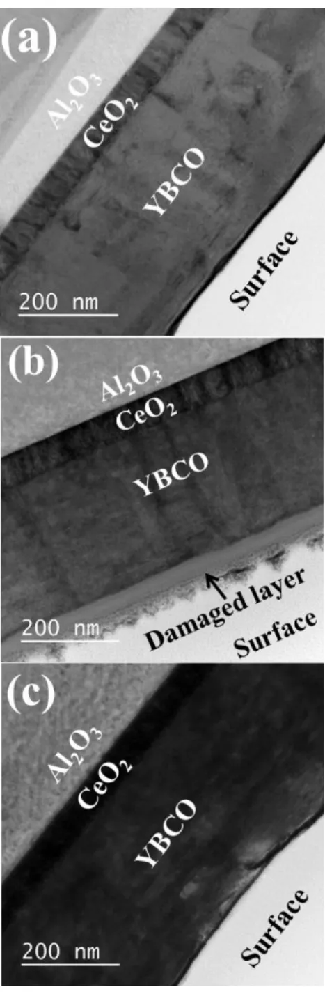
Fig. 7(a) shows TEM images for the cross section of (a) non-irradiated and irradiated films at doses of (b) 2.2 × 10 16 e/cm 2 and (c) 7.5 × 10 16 e/cm 2 . As can be seen in all samples, YBCO was well grown on an Al 2 O 3 single crystal substrate with a CeO 2 buffer layer. The thickness of the grown YBCO layer is approximately 300 nm and the CeO 2 buffer layer is 65 nm. The surface of the non-irradiated YBCO film is quite clean (Fig. 7(a)). In comparison with film (a), new layers were observed to have formed near the surfaces of films in Fig. 7(b). Layers with a thickness of 50 nm are continuous in parts of the films and are sometimes localized (see Fig. 7(b)).
The thin layers appear to be formed through EB irradiation.
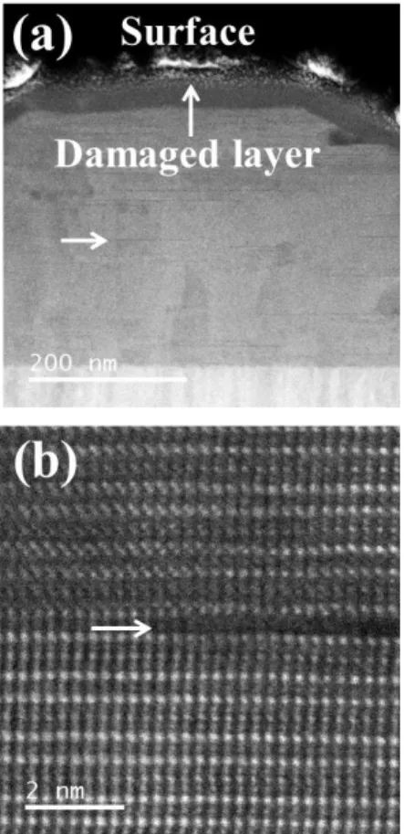
For a better understanding of the microstructures near the
damaged layer, a high-resolution TEM analysis was carried out for the same films. The lattice image of the
non-irradiated film in Fig. 8(a) shows the regularly stacked
crystal lattice. It is difficult to find the lattice defects such as
point defects, dislocations and stacking faults in the film.
Compared with the non-irradiated film, many defects were observed in the damaged layers near the film surfaces. As shown in the high-magnification TEM images for the region near the damaged layer of the film (Fig. 8(b)), the interior of the film is a crystalline phase, whereas the region near the film surfaces is amorphous.
The EB irradiation seems to destroy the crystallinity of
0 1 2 3 4 5
10
510
610
710
8Non-irradiation 7.50
15e/cm
22.210
16e/cm
25.210
16e/cm
27.510
16e/cm
2