DOI: http://dx.doi.org/10.4313/JKEM.2015.28.11.683 ISSN 1226-7945 (Print), 2288-3258 (Online)
비정질 및 단결정 실리콘에서 10∼50 keV 에너지로 주입된 안티몬 이온의 분포와 열적인 거동에 따른 연구
정원채a
경기대학교 전자공학과
A Study on Implanted and Annealed Antimony Profiles in Amorphous and Single Crystalline Silicon Using 10 ∼50 keV Energy Bombardment
Won-Chae Jung
aDepartment of Electronic Engineering, Kyonggi University, Suwon 16227, Korea
(Received October 2, 2015; Revised October 23, 2015; Accepted October 24, 2015)
Abstract: For the formation of N+ doping, the antimony ions are mainly used for the fabrication of a BJT (bipolar junction transistor), CMOS (complementary metal oxide semiconductor), FET (field effect transistor) and BiCMOS (bipolar and complementary metal oxide semiconductor) process integration. Antimony is a heavy element and has relatively a low diffusion coefficient in silicon. Therefore, antimony is preferred as a candidate of ultra shallow junction for n type doping instead of arsenic implantation. Three-dimensional (3D) profiles of antimony are also compared one another from different tilt angles and incident energies under same dimensional conditions. The diffusion effect of antimony showed ORD (oxygen retarded diffusion) after thermal oxidation process. The interfacial effect of a SiO2/Si is influenced antimony diffusion and showed segregation effects during the oxidation process. The surface sputtering effect of antimony must be considered due to its heavy mass in the case of low energy and high dose conditions. The range of antimony implanted in amorphous and crystalline silicon are compared each other and its data and profiles also showed and explained after thermal annealing under inert N2
gas and dry oxidation.
Keywords: Antimony implantation, ORD, Diffusion, Sputtering, Computer simulation
1. 서 론
안티몬은 ultra shallow extension 형성을 위한 buried layer, punch-through 방지, well doping의
a. Corresponding author; [email protected] Copyright ©2015 KIEEME. All rights reserved.
This is an Open-Access article distributed under the terms of the Creative Commons Attribution Non-Commercial License (http://creativecommons.org/licenses/by-nc/3.0) which permits unrestricted non-commercial use, distribution, and reproduction in any medium, provided the original work is properly cited.
dopant로서 As보다 더 우수하다. Sb 이온 주입을 통
해서 sub-100 nm MOSFET를 위한 매우 낮은 저항
을 형성하는 ultra shallow p-n 접합을 제작할 수가
있다. 본 연구에서는 낮은 에너지(10∼50 keV)로 주입된
Sb의 수직 및 수평 분포가 300 Å 이하로 나타나는
ultra shallow 접합 분포를 알 수가 있고, 향후에 nano
scale 의 소자 제작에 적용될 수 있는 신뢰할 수 있는 공
정 조건을 확립할 수 있다고 사료된다. 이온 주입량 즉,
dose가 1×10
15cm
-2보다 더 높은 경우에는 precipitation
2. 실험 방법
2.1 모의실험 및 해석
2.1.1 컴퓨터 시뮬레이션을 통한 안티몬 이온 주입 된 실리콘 기판의 물리적인 특성 분석
2.1.1.1 T-dyn 시뮬레이션으로 부터 안티몬 이온 주입된 실리콘 기판의 sputtering 특성 조사
그림 1은 SRIM [4,5] 데이터로서 에너지 E=170 keV에 서 핵정지력 (S
n)이 최대로 나타나기에 sputtering이 최 대로 일어나는 에너지로 판단할 수가 있는 반면에 전자 정지력 (S
e)은 1 eV에서 10 MeV까지 에 비례하는 꾸준히 증가하는 형태의 전자 정지력을 나타내고 있다.
실리콘 기판에 10∼50 keV의 에너지로 가속된 안티몬 이온의 분포와 sputtering 효과와 열처리 후에 안티몬 이온의 거동에 대해서 연구하였다. SRIM, T-dyn [6,7], ICECREM [8,9], UT-Marlowe [10,11] 컴퓨터 시뮬레 이션을 통하여 단결정 및 비정질 실리콘에서 안티몬 이 온의 분포와 range 데이터를 서로 비교 분석하였다.
Fig. 1. Electronic and nuclear stopping power of antimony implanted in silicon from various energy between 0.1 keV and 105 keV.
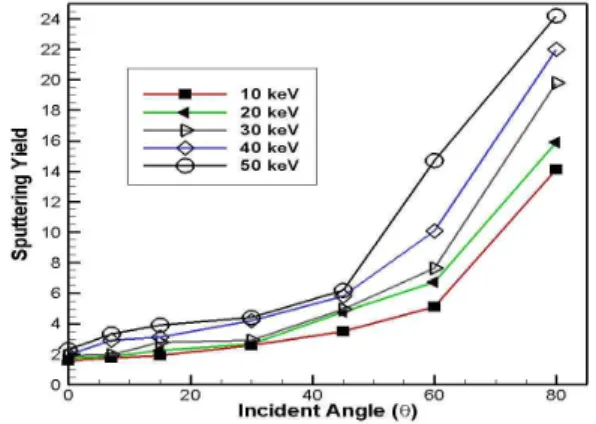
Fig. 2. Sputtering yield from different incident angles and energies using antimony implantation with a dose of 1×1014 cm-2 in silicon.
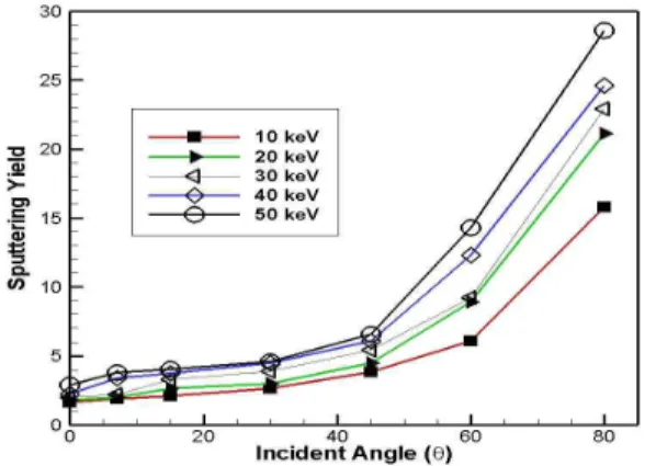
Fig. 3. Sputtering yield from different incident angles and energies using antimony implantation with a dose of 1×1015 cm-2 in silicon.
Sputtering 효과에 의한 표면 부식층 두께(
)는 수식 (1)과 같이 나타낼 수 있다.
(1)
여기서 S는 sputtering yield이고, N는 target의 density이고, 는 dose를 각각 나타낸다.
가 일정 한 경우 주입된 이온의 농도 분포는 가우스 분포로 수 식 (2)와 같이 나타낼 수가 있다.
∆
∆
(2)
Fig. 4. Sputtering yield from different incident angles and energies using antimony implantation with a dose of 1×1016 cm-2 in silicon.
일반적으로 n 타입 도핑을 위해서 1×10
14cm
-2에서 1×10
16cm
-2으로 안티몬 이온의 서로 다른 주입량 (dose) 에 따른 sputtering yield를 이온 주입 각도와 에너지에 대해서 T-dyn의 시뮬레이션을 통하여 그 결과를 그림 2에 서 4까지 각각 나타내었다. 그림 2와 3과는 달리 Sb의 이 온 주입량이 증가함에 따라서 sputtering yield가 다소 증 가하여서 그림 4에서 y축의 스케일이 다소 더 큰 값으로 나타남을 확인하였다. 안티몬이 10 keV의 에너지에서 이온 의 주입량이 1×10
15cm
-2인 경우에 실리콘 표면에서 대략 20 Å 정도가 sputtering되어 나타나는 결과를 나타내었다.
2.1.1.2 SRIM 시뮬레이션으로 부터 실리콘 기판에 이온 주입된 안티몬의 농도 분포
그림 5에서 그림 11은 몬테카를로 시뮬레이션 툴인 SRIM 2013 [5]을 이용하여 에너지 20 keV에서 입사 각 도가 0°에서 80°로 이온 주입하였을 때에 나타나는 3차 원의 Sb의 농도 분포를 나타내고 있다.
Fig. 5. Antimony 3D distribution implanted in silicon at 0°.
Fig. 6. Antimony 3D distribution implanted in silicon at 7°.
Fig. 7. Antimony 3D distribution implanted in silicon at 15°.
Fig. 8. Antimony 3D distribution implanted in silicon at 30°.
Fig. 9. Antimony 3D distribution implanted in silicon at 45°.
Fig. 10. Antimony 3D distribution implanted in silicon at 60°.
Fig. 11. Antimony 3D distribution implanted in silicon at 80°.
수직방향의 길이는 800 Å이고, 측면의 길이는 수직 방향의 반이 되는 400 Å이다. 입사 각도가 0°에서 80°
로 커짐에 따라서 수직방향의 침투 분포는 얕아지고 측 면방향으로 안티몬 이온의 분포가 더 넓게 퍼짐을 확인 할 수가 있다.
2.1.2 입사 각도, 에너지 및 열처리에 따른 컴퓨터 시뮬레이션 결과
0° 입사각으로 즉 channeling 각도로 안티몬 이온 을 비정질 실리콘에 이온 주입한 경우가 단결정 실리 콘에 이온 주입한 것보다 그림 12에서 나타난 결과처 럼 R
p및 △R
p의 값이 더 크게 나타남을 확인할 수 있 었다. 이 이유는 안티몬이 상대적으로 heavy 이온이고 또한 이온의 분포가 비정질 기판에서 전형적인 gauss 분포를 나타내어 상대적으로 단결정 실리콘 기판에서 보다 더 광범위한 분포를 나타내기 때문이다.
그림 13과 14는 비정질 실리콘 결정과 단결정질 실 리콘 기판에서 안티몬 주입에너지가 10 keV에서 50 keV의 범위에서
121Sb 이온 주입 입사각이 7°에서 80°로
Fig. 12. Range data of antimony implanted in silicon from various energy between 20 and 50 keV at 0° incident.
Fig. 13. Rp of antimony implanted in silicon from various energy between 10 and 50 keV from 7° to 80° incident angle.
Fig. 14. △Rp of antimony implanted in silicon from various energy between 10 and 50 keV from 7° to 80° incident angle.
변할 때에 안티몬의 R
p와 △R
p의 값을 서로 비교하여
나타내었다. 그림의 오른쪽에서 숫자는 서로 다른 입사
각들을 나타내고 있다. 그래프의 위에서 아래 방향으로
두 개의 선을 서로 비교해 보면, 비정질 실리콘 기판에
Fig. 15. Profiles of antimony implanted in silicon from various energy between 10 and 50 keV at 0° incident angle.
서의 R
p와 △R
p의 값이 단결정 실리콘에서 보다 더 큰 값을 나타내어서 안티몬 이온의 분포가 비정질 실리콘 기판에서 최대 농도 값을 중심으로 광범위한 damage 효과가 나타나서 폭 넓게 가우스 분포 형태의 결과를 나 타내고 있다.
그림 15는
121Sb 이온 주입 수직 입사 즉 0° 각도인 channeling 조건에서 안티몬의 농도 분포를 나타내고 있다. 비정질 실리콘 기판에서 안티몬의 분포가 단결정 실리콘 기판에서의 분포보다 상대적으로 heavy 이온이 기에 damage 영역이 축척되어 보다 더 폭 넓게 퍼져있 음을 확인할 수가 있다.
그림 16은 가속에너지가 10 keV이고, 주입량이 1×10
14cm
-2이고, 이온 주입 후에 질소가스에서 열처리, 건식산화로 열처리한 경우들에 대한 안티몬의 농도 분포를 각각 나타내 고 있다. RTA (rapid thermal annealing)인 경우는 N
2분 위기에서 1,000°C, 1분간의 급속 열처리한 경우이고 노 열처 리 (furnace annealing)의 경우는 800°C 에서 30분간 열처 리를 각각 수행한 결과이다. 건식 산화(dry oxidation)를 통 한 열처리의 경우도 마찬가지로 두 가지 경우로 RTA 와 furnace 열처리를 과정을 수행하여 그림 16에 나타내었다.
이때에 단결정 실리콘에 질소분위기에서 RTA 1분은 CRY-RTA로 노 열처리는 CRY-FUR로, 비정질 실리콘 기판에서는 RTA-SRIM, FUR-SRIM 으로 각각 나타내었 다. 또한 건식산화 후에 RTA로 1분간 열처리한 SiO
2막의 두께는 44.6 Å이었고 DRY-RTA-SRIM으로 나타내었고, 노 열처리로 800°C에서 30분간 열처리한 경우 SiO
2막의 두께는 48 Å을 나타내었다. 이 경우에 DRY-FUR-SRIM 으로 표기하였다. 이때에 최대 농도의 값, 즉 C
peak와 그 때의 침투 깊이 X
j를 각각 표 1에 자세히 나타내었다.
Fig. 16. Profiles of antimony implanted in silicon from various energy between 10 keV at 0° incident angle.
Table 1. Results from the ICECREM, UT-Marlowe, and SRIM simulation data for 10 keV 121Sb+ implantation in amorphous and crystalline silicon.
Model Xj (μm) Cpeak (cm-3)
CRY-RTA 0.0159 7.47×10¹⁹
CRY-FUR 0.0155 8.89×10¹⁹
DRY-RTA-CRY 0.0154 4.62×10¹⁹ DRY-FUR-CRY 0.0145 8.46×10¹⁹ RTA-SRIM 0.0186 6.77×10¹⁹ FUR-SRIM 0.0183 7.59×10¹⁹ DRY-RTA-SRIM 0.0178 4.47×10¹⁹ DRY-FUR-SRIM 0.0173 7.37×10¹⁹
붕소나 인의 확산이 틈새(interstitials)로 확산하는 반 면에 Sb은 공공(vacancy)의 메커니즘에 의해서 주로 확 산한다. 산화 동안에 주입된 틈새는 실리콘 bulk에서 공 공과 재결합한다. 또한, 공공농도를 억압하면서 Sb확산 을 방해하게 된다.
표 1에서 나타나 있듯이 건식산화 후에 ORD (oxide retarded diffusion) 효과 때문에 산화 막을 제거한 후 에 C
peak의 위치는 표면 쪽 방향으로 더 치우쳐 있음을 확인할 수 있었다.
3. 결과 및 고찰
그림 15와 16 및 표 1에서 나타낸 결과로 부터 10
keV
121Sb
+의 경우에 C
peak의 위치는 열처리 전에는 94
Å에서 RTA 열처리 후에는 159 Å으로 나타나는 매우
얕은 접합 분포를 나타내었다. 또한 건식산화 1,000°C에
50 77 88 117 188 255 307 346
서 RTA 1분 후에서는 3.3%, 800°C에서 30분간 노 열 처리에서는 6.9%로 최대 농도의 위치가 표면 쪽으로 이 동하는 ORD의 효과를 확인할 수 있었다. 반면에 비정질 실리콘 기판으로 Sb 이온 주입 후에 열처리한 경우는 비 정질 실리콘이 620°C 이상의 온도에서 다결정 실리콘으 로 변하여 grain boundary를 따라서 확산을 나타내기 때문에 확산이 더 빨리 일어나고 확산계수의 값이 800°C 에서 3.6×10
-11cm
2/s이고, 1,000°C에서는 1.1×10
-9cm
2/s를 나타내었다. 단결정 실리콘 기판에서의 Sb의 확산계수는 다소 더 작은 값인 800°C에서 7.9×10
-14cm
2/s이고, 1,000°C에서 1.6×10
-12cm
2/s를 각각 나타 내었다. 확산에 따른 시뮬레이션 결과인 그림 16과 잘 일치함을 확인하였다. 건식산화 동안에 산화 막과 실리 콘의 경계면에서 pile up이 나타나고 Sb의 trapping이 나타난다. 열처리가 진행됨에 따라서 pile up이 일어나 고 실리콘에서 mobile Sb는 확산이 감소하는 결과를 나 타나게 된다. Sb은 상대적으로 As보다 확산계수가 더 크기 때문에 ultra shallow p-n 접합을 형성할 수가 있다. 또한 pile up 효과는 짧은 열처리 시간을 가지는 RTA에 의해서 억압할 수가 있다.
표 2에서 측면 방향의 분포인 △R
L의 시뮬레이션 결 과로 에너지와 입사 각도가 커짐에 따라서 안티몬의 분 포가 수직방향의 분포보다도 측면방향으로 더 퍼지는 분 포를 나타내었다.
4. 결 론
실리콘 기판에서 에너지 10 keV, 주입량 1×10
14cm
-2으로 이온 주입하였다. 800°C에서 1,100°C까지 건식산화 1분간 RTA 열처리 한 경우와 30분간 노 열처리한 경우 에도 SiO
2막의 두께와 상관없이 분리계수는 거의 일정 한 10의 값을 나타내었다. 에너지 10 keV로 Sb 이온 주
시뮬레이션을 통하여 나타내었다. 입사 각도가 더 기울어 짐에 따라서 수직방향의 분포보다 측면방향의 Sb 이온분 포가 더 많이 나타나기 때문에, 표면방향으로 더 치우치 는 분포를 그림 13과 표 2에서 확인하였다. 또한, 입사 각도와 에너지에 따른 Sb의 range를 그림 13과 그림 14에 각각 나타내었다.
표 1과 그림 16에서 나타낸 것처럼 건식산화 공정 후에 ORD 효과 때문에 산화 막을 제거한 후에 C
peak의 위치는 표면 쪽 방향으로 더 치우쳐 있음을 확인할 수 있었다. 이 이유는 건식산화 동안에 segregation 효과 때문에 SiO
2/Si 경계면에 pile-up 효과가 나타나 고, Sb의 trapping이 나타나서 높은 dose인 경우에 precipitation을 일으키고 확산을 방해하는 ORD 효과 가 나타남을 확인하였다. 또한, precipitation에 대한 자세 한 현상을 규명하기 위해서는 서로 다른 에너지에서 1×10
15cm
-2보다 더 높은 dose로 이온 주입 실험을 수행하여서 TEM (transmission electron microscopy) 및 SIMS (secondary ion mass spectroscopy) tool을 사용하여 열 처리 전후의 결과를 바탕으로 물리적 및 전기적인 특성들을 서로 비교 분석한 다양한 연구가 필요한 실정이다.
본 연구의 data는 낮은 에너지(10∼50 keV)로 주입된 Sb의 수직 분포가 200 Å 이하로 수평 분포가 300 Å 이하로 나타나는 ultra shallow 접합 분포를 알 수가 있 고 신뢰할 수 있는 컴퓨터 시뮬레이션 공정 조건을 확립 할 수 있다고 사료된다.
REFERENCES
[1] T. Alzanki, K. M. Kandil, N. Bennett, B. J. Sealy, M. R.
Alenezi, A. Almeshal, M. Jafar, and A. Ghoneim, SOJ Mat. Sci. Eng., 2, 1 (2014).
[2] N. S. Benett, N. E. B. Cowern, A. J. Smith, R. M.
Gwilliam, B, J. Sealy, L. O’Reilly, P. J. McNally, G.
Cooke, and H. Kheyrandish, Appl. Phys. Lett., 89, 182122 (2006). [DOI: http://dx.doi.org/10.1063/1.2382741]
[3] R. Low, B. J. Sealy, and R. Gwilliam, J. Appl. Phys., 95, 5471 (2004). [DOI: http://dx.doi.org/10.1063/1.1702096]
[4] J. F. Ziegler, J. P. Biersack, and U. Littmark, The Stopping and Range of Ions in Solids (Pergamon, New York, 1985).
[5] J. F. Ziegler, SRIM 2013 Manual, http://www.srim.org/.
[6] W. Möller and W. Eckstein, Nucl. Insrum. Methods B, 2, 814 (1984). [DOI: http://dx.doi.org/10.1016/0168-583X(84)90321-5]
[7] W. Eckstein, Computer Simulation of Ion-Solid Interactions (Springer, Berlin 1991).
[DOI: http://dx.doi.org/10.1007/978-3-642-73513-4]
[8] H. Ryssel, J. Lorenz, and W. Kreuger, Nucl. Insrum.
Methods, B19, 45, (1987).
[DOI: http://dx.doi.org/10.1016/S0168-583X(87)80012-5]
[9] User's Guide, ICECREM Manual (1996).
[10] C. Park, K. M. Klein, and A.L.F. Tasch, Solid State Electonics, 33, 645 (1990).
[DOI: http://dx.doi.org/10.1016/0038-1101(90)90176-F]
[11] C. Park, K. M. Klein, and A.L.F. Tasch, IEEE Trans.
Electron Dev., 39, 1614 (1992).
[DOI: http://dx.doi.org/10.1109/16.141226]