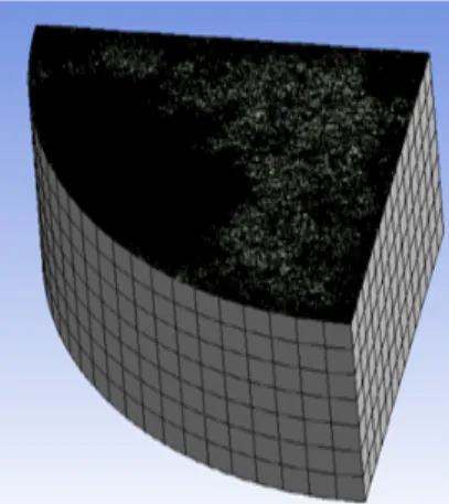
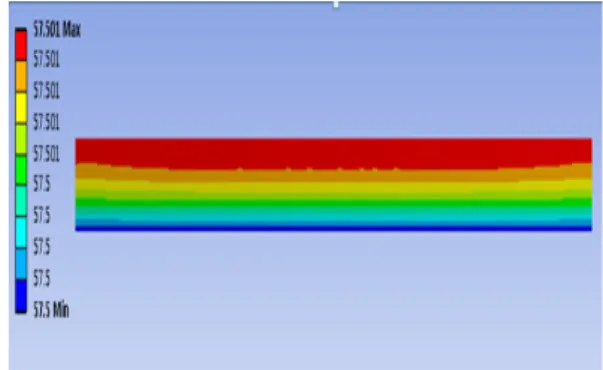
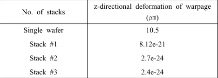
Warpage Simulation by the CTE mismatch in Blanket Structured Wafer Level 3D packaging
5
0
0
전체 글
(2)
(3)
(4)
(5)
수치

관련 문서
