Design of a Dual mode Three-push Tripler Using Stacked FETs with Amplifier mode operation
Hong-sun. Yoon, Youngcheol. Park *
Abstract
In this paper, we propose a dual-mode frequency tripler using push-push and stacked FET structures. The proposed circuit can operate either in frequency multiplier mode or in amplifier mode. In the frequency multiplier mode, push-push frequency multiplication is achieved by allowing input signals with particular phase shifts. In the amplifier mode, the device operates as a distributed amplifier to obtain high gain. Also both modes were designed using stacked FET structure. The designed circuit showed frequency tripled output power of 9.7 dBm at 2.4 GHz with the input at 800 MHz. On the other hand, in the amplifier mode, the device showed 8.9 dB of gain to generate 19.5 dBm at 800 MHz.
Key words:Frequency multiplier, N-pushing structure, Dual-mode, Dual band, Stacked FET, Distributed amplifier
* Dept. of Electronics Engineering, Hankuk University of Foreign Studies.
★ Corresponding author
E-mail:[email protected], Tel:+82-31-330-4972
※ Acknowledgment
This research was supported by Hankuk University of Foreign Studies Research Fund, and Basic Science Research Program through the National Research Foundation of Korea(NRF) funded by the Ministry of Education (2017R1D1A1B03032874).
Manuscript received Dec. 7, 2018; accepted Dec. 22, 2018; accepted Dec. 26, 2018
This is an Open-Access article distributed under the terms of the Creative Commons Attribution Non-Commercial License (http://creativecommons.org/licenses/by-nc/3.0) which permits unrestricted non-commercial use, distribution, and reproduction in any medium, provided the original work is properly cited.
Ⅰ. Introduction
In this paper we propose a new circuit that is a dual mode push-push frequency tripler. The circuit operates in dual modes: an amplifier mode with a distributed amplifier structure that amplifies 800 MHz input signals; a frequency multiplier mode that triples input signals into higher frequency. The operation frequencies are chosen as 800 MHz and 2.4 GHz in consideration of the ISM and TRS (Trunked Radio System) operation.
While there exist many methods that support dual-band operation of wireless devices, mixer-free approach has been studied as an alternate way to conventional up/down conversion method. One of the topology was suggested to use active frequency dividers, from which 0.8 GHz output is generated
by utilizing an active frequency divider on 2.4 GHz signal [1], [2]. In this regard, a structure that multiplies low frequency components but with less phase noise [3] might be a good candidate for multi-band frequency operation, which is suggested in this paper.
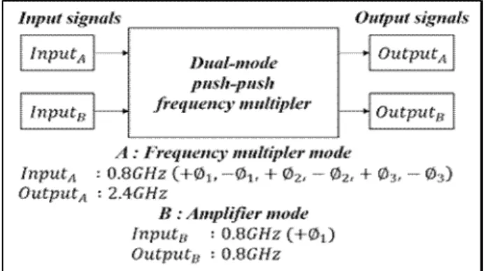
Fig. 1. Block diagram of the proposed dual-mode frequency tripler.
203
The block diagram of the proposed dual-mode frequency tripler is illustrated in Fig. 1. In amplifier mode, the circuit operates as a conventional amplifier at 0.8 GHz.
Second, in frequency multiplier mode, the carrier frequency is tripled into 2.4 GHz. However, the frequency multiplication process loses gain by nature, and conventionally additional amplifier is required at the output [4].
In this paper, in order to supply more gain in the frequency multiplier mode, this paper deployed stacked FET architecture, which is discussed in Section 2. Section 3 is about the detailed circuit design for switching between modes with circuit simulation result. Section 4 gives the conclusion and discussion.
Ⅱ. Principle about N-Push technique
2.1. Frequency multiplier
Commonly, frequency conversion circuit is used for mixers, but it has a large circuit size. This gets worse when multi-frequency operation is required by the system. Therefore, in order to save the circuit area for the frequency conversion and to support dual-band, the author has suggested circuits that is based on frequency multiplier architecture [5]. One way of achieving frequency multiplication is to use a harmonic component of nonlinear transistors. But this approach must use filter to reject unwanted output signals. In addition, it needs extra amplifiers to boost the output signal.
The other way to multiply frequency is to use the N-push technique. The N-push technique does not require additional amplifiers and filters because the desired harmonic components are constructively added together and the unwanted low order harmonic components are cancelled out [6], [7]. In this work, we used this N-push frequency multiplier in order to simplify the circuit.
2.2. N-Push technique
In this structure, there are two major structures
such as cascade structure and parallel structure.
Although they share the same aforementioned advantage, the push-push structure does not require extra blocks such as doubler, amplifier and filter, and this leads to a simpler circuit structure.
This push-push structure can extend to an N
thharmonic controlled structure. For the extension, the circuit needs to arrange N input sources and transistors with a proper phase relation. The N input sources are used to produce N signals with 2π/N phase difference between adjacent elements.
Behind the input sources, each path is connected to phase shifters to control the conductive angle of the output signal.
In this paper, this push-push structure is extended to a tripler. Hence, it needs three input sources with the phase of 2π/3 difference between adjacent elements, and corresponding transistors.
There is a phase shift of 2π/3 among three fundamental signals. The second harmonic signal has a phase shift of 4π/3, while the 3rd harmonic signal has a phase shift of 2π. It means that the fundamental and the second harmonic signals will cancel themselves out and the 3rd harmonic signal (the desired output signal) will combine in phase [8].
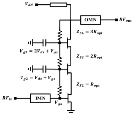
2.3. FET stacking topology
CMOS FETs in general have low breakdown voltage, which leads to relatively low gain in amplifiers. As such, FET-stacking technique is used to overcome the drawback as shown in Fig.
2 [9]. This topology is composed of a series
connection of a common source transistor and
two likely common gate transistors. This circuit
can be misunderstood as a common gate, but
unlike the cascode structure, in which the input
of the common gate transistor is processed by
RF-ground, the circuit of the stacked FET has
an appropriate external capacitor at the gate of
each FET, which creates RF swings between
gate-source and drain-source. This can solve the
gate drain breakdown voltage problem that occurs in the common gate of the cascode and makes it possible to use a high drain voltage.
Stacked transistor’s input source impedance values very important because they determine the gate bias.
Assuming that is very large, and in the low RF frequency range, the source input impedance
of a stacked transistor can be defined as
×
≈
×
(1)
And, of each source input impedances correspond to of each transistor [10]. As a result, it is possible to obtain an output signal with proper gain.
IMN
OMN
= +
= +
=
=
=
Fig. 2. Structure of stacked FET PA.
Ⅲ. Circuit Design
3.1. Operation in Frequency Multiplier Mode The -push multiplier can generate N
thharmonic without low-order 2
nd~(N
th-1) harmonic components.
The ideal output signal of the N input sources is the square wave. Assuming all harmonics have the same time delay. The combined output signal is expressed as follows:
≈ π ∙ ∙ ω (2)
where A is the signal amplitude and t
d,kis the time delay of the k
thoutput.
Frequency multiplication is applied to the input signal to have a phase difference expressed as follows:
∅
π × ⋯ (3)
In this circuit, we apply time delay to input sources in order to achieve phase offset as follows:
∅
π
∙ → ∅
∙
π
∙
π ∙
∴
∙
×
×
(4)
Applying time delay between the input signals can be implemented outside the package through the transmission line on a printed circuit board.
In this work, we used differential cascade structure so that it does not require additional matching circuits. The conventional N-push multiplier circuit consists of distributed amplifiers (M1~M6) as shown in Fig. 3, in which transistor (M1~M3) are for the positive input signals with proper time delays, whereas transistor (M4~M6) are for the negative input signals.
Fig. 3. Circuit of three-push tripler.
As a result, the output is switching at three
times the input frequency. Fig. 4 shows the
result of the operation in the frequency multiplier
mode. Its period is 0.417 ns, which represents the
frequency of 2.4 GHz. However, as can be
observed, the amplitude of the output signal is
reduced compared to the input signal.
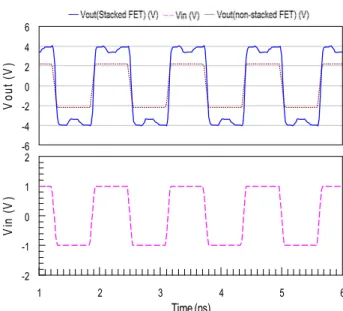
In order to compensate for this gain loss, this paper circumvents the problem by stacking additional transistors on the conventional multiplier structure. Fig. 5 shows the proposed structure, in which transistors (M7~12) are stacked on top of the existing push-push frequency multiplier structure. And it can operate in dual mode by using SPDT and phase shifters. Fig. 6 shows the result of comparison between the conventional frequency multiplier and the frequency multiplier with the stacked FET structure. As shown in the figure, the structure using stacked FET technology has a voltage gain of 3.34 dB in contrast to negative gain of the conventional push-push case.
1 2 3 4 5 6
Time (ns) -1
-0.5 0 0.5 1
Vout (V)
Fig. 4. Result of frequency multiplier mode.
120o 120o 120o 120o
SPDT
~ ~ -+
+-
+ Vout-
M1 M2 M3 M6 M5 M4
M7 M8 M9 M12 M11 M10
VDD
SPDT SPDT SPDT SPDT SPDT
RL
RL
Fig. 5. Circuit of dual mode tripler using stacked FETs.
Also, by using the stacked FET structure, it can be expected that the impedance of the final load stage increases and the matching with the output stage is simpler, which can save additional loss from the output impedance transformer circuit.
3.2. Operation in Amplifier mode
External SPDT (Single pole, double throw) element is used to switch between the circuit modes. In the amplifier mode, input signals of the same phase are applied by the SPDT control to show the operation of a distributed amplifier.
In general, gain is doubled by doubling the transistor width, but this doubling the width decrease the bandwidth due to the increased parasitic capacitance. But in this amplifier, cascade transistors are arranged in parallel to amplify the magnitude of the output current without degrading the bandwidth. So, higher gain and better bandwidth are still expected.
1 2 3 4 5 6
Time (ns)
-2-1 0 1 2
V in ( V )
-2 -1 0 1 2