Regular Paper 521 J. KIEEME
Vol. 25, No. 7, pp. 521-524, July 2012
DOI: http://dx.doi.org/10.4313/JKEM.2012.25.7.521
활성층 두께 및 열처리 온도에 따른 비정질 인듐갈륨징크옥사이드 박막트랜지스터의 전기적 특성 변화
백찬수
1
, 임기조1
, 임동혁2
, 김현후2,a
1 충북대학교 전기공학부
2 두원공과대학교 디스플레이공학부
Electrical Properties Depending on Active Layer Thickness and Annealing Temperature in Amorphous In-Ga-Zn-O
Thin-film Transistors
Chan Soo Baek
1, Kee Joe Lim
1, Dong Hyeok Lim
2, and Hyun-Hoo Kim
2,a1
College of Electrical Engineering, Chungbuk National University, Cheongju 361-763, Korea
2
Display Engineering School, Doowon Technical University College, Paju 413-861, Korea
(Received June 14, 2012; Revised June 21, 2012; Accepted June 24, 2012)
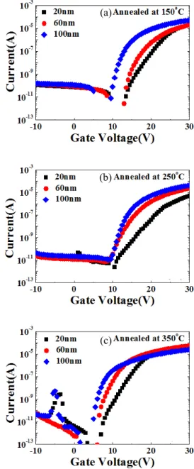
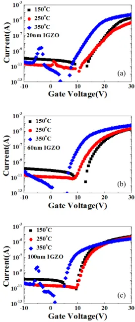
Abstract: We report on variations of electrical properties with different active layer thickness and post-annealing temperature in amorphous In-Ga-Zn-O (IGZO) thin-film transistors (TFTs). In particular, subthreshold swing (SS) of the IGZO-TFTs was improved as increasing the active layer thickness at an given post-annealing temperature, accompanying the negative shift in turn-off voltage. However, as increasing post-annealing temperature, only turn-off voltage was shifted negatively with almost constant SS value. The effect of the active layer thickness and post-annealing temperature on electrical properties, such as SS, field effect mobility and turn-off voltage in IGZO-TFTs has been explained in terms of the variation of trap density in IGZO channel layer and at gate dielectric/IGZO interface.
Keywords: Active layer, In-Ga-Zn-O, Trap, Annealing, Thickness